Voltage regulation circuit and method and display device
A voltage adjustment circuit and voltage compensation technology, applied in static indicators, instruments, etc., can solve the problems of abnormal picture and difficult inversion of liquid crystal molecules, and achieve the effect of simplifying the circuit structure
- Summary
- Abstract
- Description
- Claims
- Application Information
AI Technical Summary
Problems solved by technology
Method used
Image
Examples
Embodiment 1
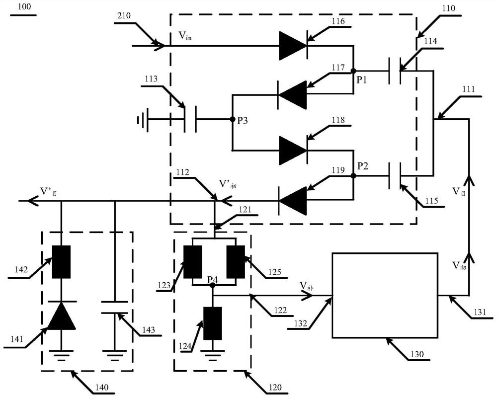
[0046] According to the first aspect of the embodiments of the present application, Embodiment 1 of the present application provides a voltage adjustment circuit 100, such as figure 1 as shown, figure 1 A circuit diagram of the voltage adjustment circuit 100 described in Embodiment 1 of the present application is schematically shown.
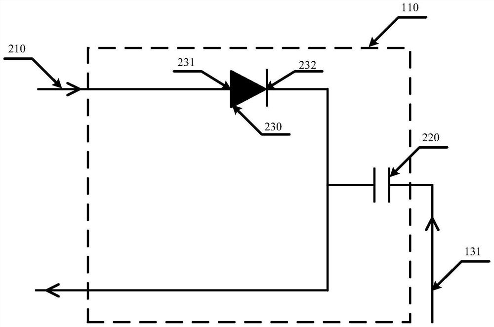
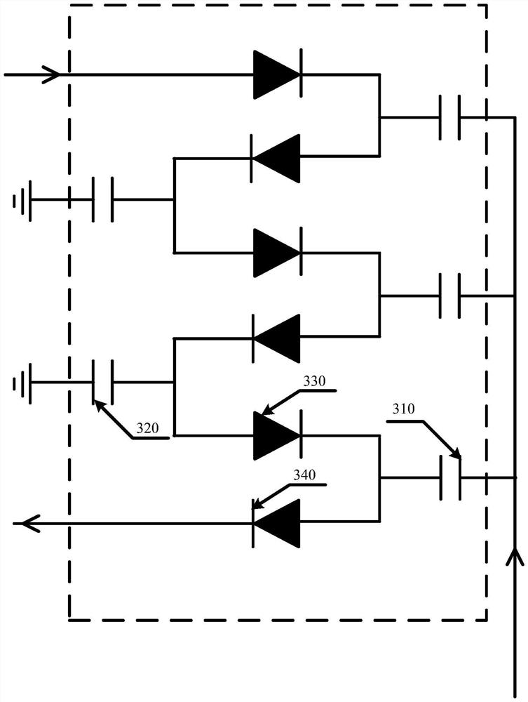
[0047] The voltage regulation circuit 100 of the present application includes a charge pump unit 110 , a voltage compensation unit 120 and a power integration unit 130 .
[0048] Wherein, the output terminal 131 of the power integration unit is connected to the input terminal 111 of the charge pump unit, and the power integration unit 130 is used to generate an initial reference voltage. The power integration unit 130 is also called a power integrated circuit (Power IC), which refers to the pulse width control integration of the switching power supply. The power supply uses the power integration unit 130 to adjust the stability of the output vo...
Embodiment 2
[0090] The above part introduces the content of the first embodiment of the present application, and then continues to introduce the content of the second embodiment of the present application. According to the second aspect of the embodiment of the present application, the present application also provides a voltage adjustment method, such as Figure 9 as shown, Figure 9 A flow chart of the voltage adjustment method described in Embodiment 2 of the present application is schematically shown. The method includes step S910-step S950.
[0091] Step S910: Using the power integrated unit to generate an initial reference voltage.
[0092] The power integration unit 130 of the present application may integrate a pulse width modulation controller, and use the pulse width modulation controller to generate an initial reference voltage, where the initial reference voltage may be a PWM square wave voltage.
[0093] Step S920: using the charge pump unit to generate an initial gate volt...
Embodiment 3
[0102] Such as Figure 10 as shown, Figure 10 A schematic diagram of the display device described in Embodiment 3 of the present application is schematically shown. This embodiment also provides a display device 1000, including a display panel 1010, a gate drive circuit 1020, and a voltage adjustment circuit 100, wherein the voltage adjustment circuit 100 is connected to the gate drive circuit 1020, and the charge pump unit of the voltage adjustment circuit 100 can The output terminal of is connected to the gate driving circuit 1020 . The gate drive circuit 1020 is connected to the display panel 1010 or the gate drive circuit 1020 is integrated on the display panel 1010 ( Figure 10 The middle gate driving circuit 1020 is set independently from the display panel 1010).
[0103] The display device of the present application can adjust the voltage of the thin film transistor to generate different gate voltages to control the inversion of the liquid crystal molecules, avoidin...
PUM
 Abstract
Description
Claims
Application Information
 - R&D
- Intellectual Property
- Life Sciences
- Materials
- Tech Scout
- Unparalleled Data Quality
- Higher Quality Content
- 60% Fewer Hallucinations
Browse by: Latest US Patents, China's latest patents, Technical Efficacy Thesaurus, Application Domain, Technology Topic, Popular Technical Reports.
© 2025 PatSnap. All rights reserved.Legal|Privacy policy|Modern Slavery Act Transparency Statement|Sitemap|About US| Contact US: help@patsnap.com


