Display panel and manufacturing method thereof

A display panel and display area technology, which is applied in the direction of instruments, electrical components, circuits, etc., can solve the problems of poor performance of red light and green light, difficulty in full-color display, and low product yield, so as to simplify the manufacturing process and ensure The effect of product yield and long life

Pending Publication Date: 2022-03-04
WUHAN CHINA STAR OPTOELECTRONICS SEMICON DISPLAY TECH CO LTD
View PDF11 Cites 3 Cited by
  • Summary
  • Abstract
  • Description
  • Claims
  • Application Information

AI Technical Summary

Problems solved by technology

[0003] Micro-led is usually formed by depositing gallium nitride material on a sapphire substrate. Due to the use of inorganic materials, there is no problem of short life and poor stability.
At present, the efficiency and lifespan of blue light Micro-led are relatively high, but the performance of red light and green light is relatively poor, and generally need to be transferred to the substrate in batches in huge quantities, resulting in a low yield rate of the obtained product, and the display realizes full Colorization is more difficult

Method used


Image

  • Display panel and manufacturing method thereof
  • Display panel and manufacturing method thereof
  • Display panel and manufacturing method thereof

Examples


Embodiment Construction

[0035] The following will clearly and completely describe the technical solutions in the embodiments of the application with reference to the drawings in the embodiments of the application. Apparently, the described embodiments are only some of the embodiments of the application, not all of them. Based on the embodiments in this application, all other embodiments obtained by those skilled in the art without making creative efforts belong to the scope of protection of this application.

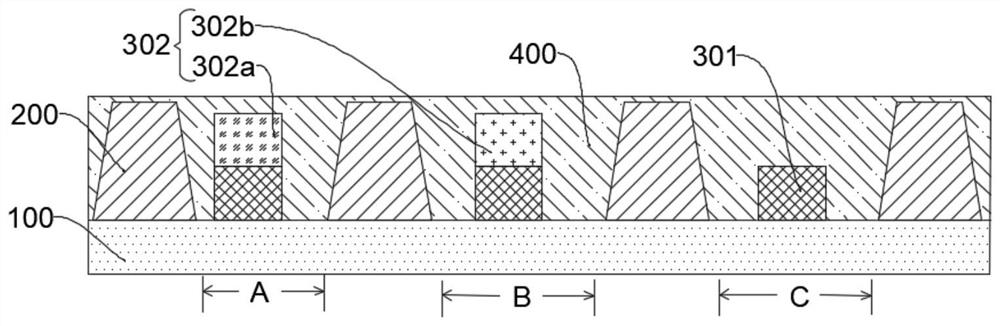
[0036] With the development of display technology, traditional human liquid crystal display technology is gradually unable to meet the needs of the market in terms of color rendering, luminous efficiency, and flexibility. The new generation of lighting and display technology has become a hot spot for investment and research. Among them, micro light-emitting diodes (micro light-emitting diodes, Micro-leds) have relatively smaller pixel sizes, and are suitable for indoor screens and small-sized di...


PUM

PropertyMeasurementUnit
refractive indexaaaaaaaaaa

Abstract

The embodiment of the invention discloses a display panel and a manufacturing method thereof. A display area of the display panel comprises a first sub-pixel area, a second sub-pixel area and a third sub-pixel area. The display panel further comprises a driving substrate, a blue light emitting device layer and a color conversion layer, and the blue light emitting device layer comprises a first blue light emitting device, a second blue light emitting device and a third blue light emitting device which are arranged on one side of the driving substrate. The color conversion layer comprises a first color conversion sub-layer arranged in the first sub-pixel region and a second color conversion sub-layer arranged in the second sub-pixel region, the first color conversion sub-layer is arranged on each first blue light emitting device, and the second color conversion sub-layer is arranged on each second blue light emitting device; according to the micro-LED display panel, the step that the blue light Micro-LED and the red light Micro-LED need to be transferred in batches and in large quantities can be effectively avoided, the service life of the red light Micro-LED and the service life of the green light Micro-LED are effectively prolonged, and the full color of the Micro-LED display panel is achieved.

Description

technical field [0001] The present application relates to the field of display technology, in particular to a display panel and a manufacturing method thereof. Background technique [0002] With the development of display technology, traditional human liquid crystal display technology is gradually unable to meet the needs of the market in terms of color rendering, luminous efficiency, and flexibility. The new generation of lighting and display technology has become a hot spot for investment and research. Among them, micro light-emitting diodes (micro light-emitting diodes, Micro-leds) have relatively smaller pixel sizes, and are suitable for indoor screens and small-sized displays. [0003] Micro-leds are usually formed by depositing gallium nitride materials on a sapphire substrate. Due to the use of inorganic materials, there is no problem of short life and poor stability. At present, the efficiency and lifespan of blue light Micro-led are relatively high, but the perform...

Claims


Application Information

Patent Timeline
Patent Type & Authority Applications(China)
IPC IPC(8): H01L33/50H01L33/00G09F9/33
CPCH01L33/504H01L33/005G09F9/33H01L2933/0041
Inventor 潘杰
Owner WUHAN CHINA STAR OPTOELECTRONICS SEMICON DISPLAY TECH CO LTD
Why Eureka
Try Eureka