A kind of array substrate and display panel

An array substrate and color filter substrate technology, applied in the display field, can solve the problems of weak electric field component, prone to TraceMura, image sticking, etc., and achieve the effect of enhancing electric field strength, reducing electric field interference, and reducing proportion

Active Publication Date: 2022-05-10
HKC CORP LTD
View PDF9 Cites 0 Cited by
  • Summary
  • Abstract
  • Description
  • Claims
  • Application Information

AI Technical Summary

Problems solved by technology

[0003] In the current IPS display mode, Trace Mura often appears, that is, after the end of the previous frame, the liquid crystal molecules cannot be deflected to the deflection state required by this frame in time, resulting in image retention, especially in the sub-pixel gate line. The edge of the pixel in the direction, because the electric field component in the horizontal direction formed between the common electrode and the pixel electrode is weaker than that in the middle of the pixel, and the electric field component in the vertical direction is stronger than that in the middle of the pixel, and the Trace Mura phenomenon is more likely to occur

Method used


Image

  • A kind of array substrate and display panel
  • A kind of array substrate and display panel
  • A kind of array substrate and display panel

Examples


Embodiment Construction

[0034] In order to make the purpose, technical solutions and advantages of the embodiments of the present invention clearer, the technical solutions in the embodiments of the present invention will be clearly and completely described below in conjunction with the drawings in the embodiments of the present invention. Obviously, the described embodiments It is a part of embodiments of the present invention, but not all embodiments.

[0035] The present application will be described in detail below with reference to the accompanying drawings and optional embodiments.

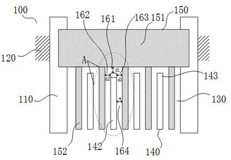
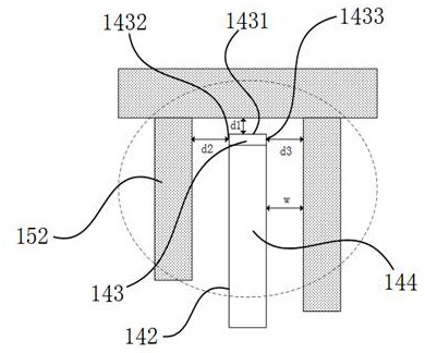
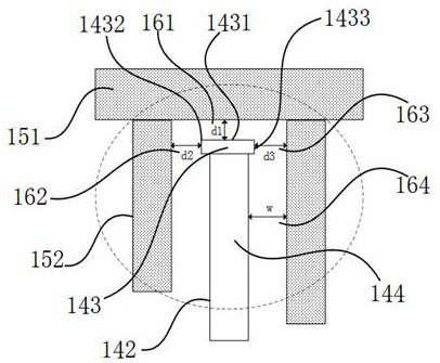
[0036] figure 1 is a schematic diagram of the array substrate of the first embodiment of the present application, figure 2 It is an enlarged schematic diagram of the branch end of the first embodiment of the present application; as figure 1 with figure 2As shown, as the first embodiment of the present application, an array substrate 100 is disclosed, including a plurality of data lines 110, a plurality of scan...


PUM


Abstract

The present application discloses an array substrate and a display panel. The common electrode layer on the array substrate includes a common electrode trunk and a plurality of common electrode branches. The pixel electrode layer includes a plurality of interconnected pixel electrode branches. The pixel electrode branch includes a branch main body and a plurality of common electrode branches. A branch end connected to the branch main body, the branch end includes a first side, a second side and a third side, the first side is arranged opposite to the common electrode trunk to form a first gap, and the second side and the third side are respectively connected to the corresponding The common electrode branches are arranged oppositely to form a second gap and a third gap; a fourth gap is formed between the branch body and the common electrode branch; among the first gap, the second gap and the third gap, at least one gap corresponds to a width value smaller than the fourth gap. The width of the gap. By narrowing the gap between the pixel electrode branch end and the common electrode, the electric field intensity at the branch end is increased, and the electric field interference between the scanning line and the data line pair between the branch end and the common electrode is reduced.

Description

technical field [0001] The present application relates to the field of display technology, and in particular to an array substrate and a display panel. Background technique [0002] With the development of display technology, the display mode of the display panel is also constantly changing, from the previous twisted nematic (TN) mode to the in-plane switching (IPS) mode. Poor vision caused by anisotropy. [0003] In the current IPS display mode, Trace Mura often appears, that is, after the end of the previous frame, the liquid crystal molecules cannot be deflected to the deflection state required by this frame in time, resulting in image retention, especially in the sub-pixel gate line. The edge of the pixel in the direction, because the electric field component in the horizontal direction formed between the common electrode and the pixel electrode is weaker than that in the middle of the pixel, and the electric field component in the vertical direction is stronger than th...

Claims


Application Information

Patent Timeline
Patent Type & Authority Patents(China)
IPC IPC(8): G02F1/1343
CPCG02F1/134309G02F1/134318G02F1/136286G02F1/134345G02F1/134363G02F1/134372G02F1/136222
Inventor 郑星龙冯纪恒卢集晖
Owner HKC CORP LTD
Why Eureka
Try Eureka