Epitaxial structure, light-emitting device and manufacturing method of epitaxial structure
A technology of epitaxial structure and fabrication method, applied in semiconductor devices, electrical components, circuits, etc., can solve the problems of difficulty in stress control of epitaxial structure, difficulty in controlling wavelength uniformity, etc.
- Summary
- Abstract
- Description
- Claims
- Application Information
AI Technical Summary
Problems solved by technology
Method used
Image
Examples
Embodiment 1
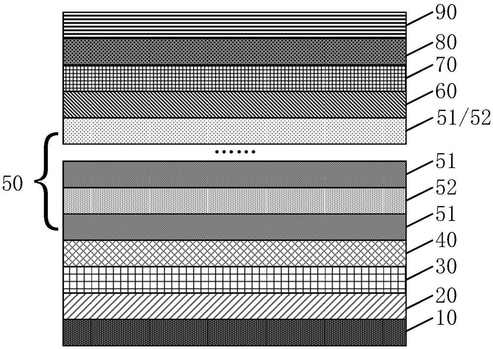
[0063] The stress release layer includes a first stress release layer 30 , a second stress release layer 40 , a third stress release layer 50 and a fourth stress release layer 60 . The first stress release layer 30 is formed on the buffer layer 20, the second stress release layer 40 is formed on the first stress release layer 30, the third stress release layer 50 is formed on the second stress release layer 40, and the fourth stress release layer 60 is formed on the third stress release layer 50 , and the N-type GaN layer 70 is formed on the fourth stress release layer 60 .
[0064] Wherein, the material of the first stress release layer 30 is AlGaN (aluminum gallium nitride), wherein the content of Al (aluminum) component is 50%-90%. Optionally, the proportion of the Al component can be 50%, 60%, 70%, 80%, 90%, etc., preferably, the proportion of the Al component is 75%.
[0065] The material of the first stress release layer 30 is AlGaN with a relatively high content of Al,...
Embodiment 2
[0083] This embodiment is basically the same as Embodiment 1, the difference is that the stress release layer only includes the first stress release layer 30, without the second stress release layer 40, the third stress release layer 50 and the fourth stress release layer 60, N type The GaN layer 70 is formed on the first stress release layer 30 .
[0084] In this embodiment, the structure, manufacturing conditions, growth thickness, and beneficial effects of the first stress release layer 30 can refer to Embodiment 1, and will not be repeated here.
Embodiment 3
[0086] This embodiment is basically the same as the first embodiment, except that the stress release layer only includes the first stress release layer 30 and the third stress release layer 50 , without the second stress release layer 40 and the fourth stress release layer 60 . Wherein, the third stress release layer 50 is directly formed on the first stress release layer 30 , and the N-type GaN layer 70 is formed on the third stress release layer 50 .
[0087] In this embodiment, the structure, manufacturing conditions, growth thickness and beneficial effects of the first stress release layer 30 and the third stress release layer 50 can refer to the first embodiment, and will not be repeated here.
PUM
| Property | Measurement | Unit |
|---|---|---|
| Thickness | aaaaa | aaaaa |
Abstract
Description
Claims
Application Information
 - R&D
- Intellectual Property
- Life Sciences
- Materials
- Tech Scout
- Unparalleled Data Quality
- Higher Quality Content
- 60% Fewer Hallucinations
Browse by: Latest US Patents, China's latest patents, Technical Efficacy Thesaurus, Application Domain, Technology Topic, Popular Technical Reports.
© 2025 PatSnap. All rights reserved.Legal|Privacy policy|Modern Slavery Act Transparency Statement|Sitemap|About US| Contact US: help@patsnap.com

