Wafer semiconductor polishing device and using method thereof

A semiconductor and wafer technology, applied in the field of wafer semiconductor grinding equipment, can solve the problems of time-consuming cleaning, inability to deal with dust in time, and affect processing efficiency, etc., achieve good filterability, avoid cumbersome subsequent cleaning, and improve grinding efficiency. Effect

Pending Publication Date: 2022-02-08
张永田
View PDF0 Cites 8 Cited by
  • Summary
  • Abstract
  • Description
  • Claims
  • Application Information

AI Technical Summary

Problems solved by technology

[0003] During the processing and production of wafer semiconductors, grinding and polishing are often required. However, in the process of grinding, it is generally necessary to manually use clamps to fix the wafer semiconductors to avoid movement during the grinding process of wafer semiconductors. However, This fixing method is cumbersome, and during the grinding process, the dust generated on the wafer semiconductor cannot be disposed of in time, so it takes time to clean the wafer semiconductor in the later stage, which greatly affects the processing efficiency

Method used


Image

  • Wafer semiconductor polishing device and using method thereof
  • Wafer semiconductor polishing device and using method thereof
  • Wafer semiconductor polishing device and using method thereof

Examples


Embodiment Construction

[0028] The following examples are for illustrative purposes only and are not intended to limit the scope of the invention.

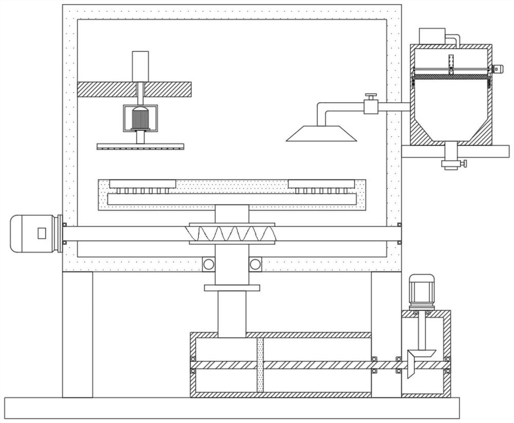
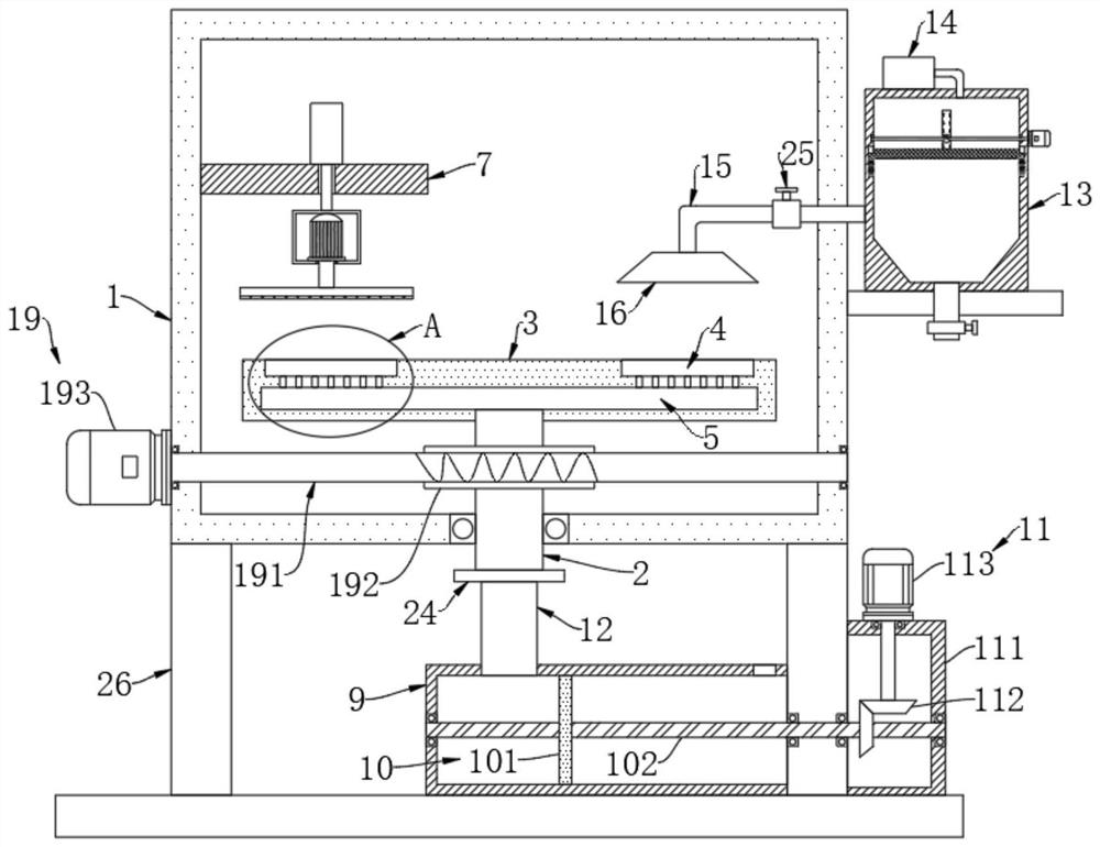
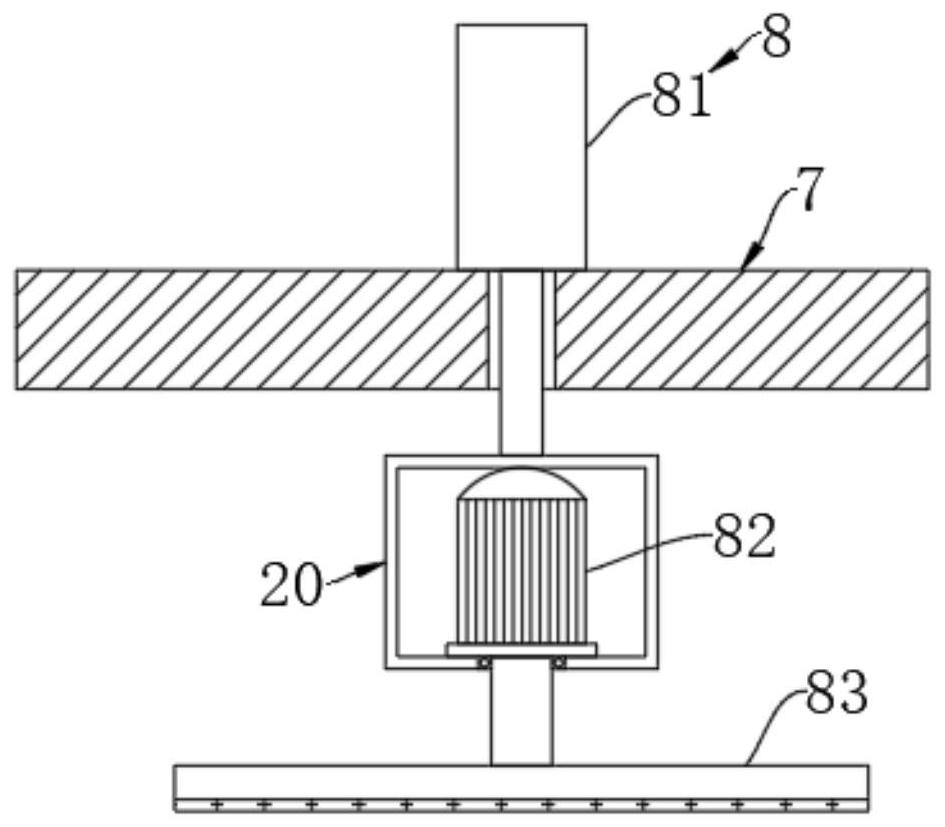
[0029] Such as Figure 1-7 As shown, a wafer semiconductor polishing device includes a polishing box 1 fixedly arranged on a support base 26, a gas pipe 2 is rotatably connected to the polishing box 1, and a fixed seat 3 is fixedly connected to the upper end of the gas pipe 2. On the fixed seat 3 A plurality of placing grooves 4 are provided, and the plurality of placing grooves 4 are distributed in a ring shape, and an air chamber 5 is provided on the fixed seat 3, and the air chamber 5 communicates with the trachea 2, and the placing groove 4 communicates with the air chamber 5 through a plurality of air holes 6 , the grinding box 1 is fixedly connected with a support plate 7, and the support plate 7 is provided with a grinding mechanism 8 matched with the placement groove 4.

[0030] The grinding mechanism 8 includes a cylinder 81, a micro motor 82 a...


PUM


Abstract

The invention belongs to the field of wafer semiconductor processing, and particularly relates to a wafer semiconductor polishing device and a using method thereof. The wafer semiconductor polishing device comprises a polishing box fixedly arranged on a supporting seat, an air pipe is rotationally connected into the polishing box, a fixing seat is fixedly connected to the upper end of the air pipe, a plurality of containing grooves are formed in the fixing seat, multiple containing grooves are annularly distributed, an air cavity is formed in the fixing seat and communicates with the air pipe, the containing grooves communicate with the air cavity through multiple air holes, and a supporting plate is fixedly connected into the polishing box. According to the wafer semiconductor polishing device, a plurality of wafer semiconductors can be fixed at the same time at a time, the complexity of manual fixing is avoided, dust generated by polishing on the wafer semiconductors can be treated in time in the polishing process of the wafer semiconductors, the complexity of subsequent cleaning is avoided, and meanwhile, the wafer semiconductor polishing device can polish a plurality of wafer semiconductors at a time, and the polishing efficiency is greatly improved.

Description

technical field [0001] The invention belongs to the field of wafer semiconductor processing, and in particular relates to a wafer semiconductor grinding device and a method for using the same. Background technique [0002] Wafer refers to the silicon wafer used to make silicon semiconductor circuits. Its raw material is silicon. High-purity polysilicon is dissolved and mixed with silicon crystal seeds, and then slowly pulled out to form cylindrical monocrystalline silicon. After grinding, polishing, and slicing, silicon wafers are formed, that is, wafers. [0003] During the processing and production of wafer semiconductors, grinding and polishing are often required. However, in the process of grinding, it is generally necessary to manually use clamps to fix the wafer semiconductors to avoid movement of the wafer semiconductors during the grinding process. However, This fixing method is cumbersome, and during the grinding process, the dust generated on the wafer semiconduct...

Claims


Application Information

Patent Timeline
Patent Type & Authority Applications(China)
IPC IPC(8): B24B7/22B24B55/06B24B27/00B24B41/06H01L21/304
CPCB24B7/228B24B55/06B24B27/0046B24B41/068H01L21/304
Inventor 张永田
Owner 张永田
Why Eureka
Try Eureka