Display panel and preparation method thereof

A technology for display panels and array substrates, applied in electrical components, electrical solid-state devices, circuits, etc., can solve the problems of blue-light Micro-LEDs with different luminous efficiency, performance and lifespan, difficulty in achieving full color, and low yield. The effect of reducing the probability of non-radiative relaxation, improving luminous efficiency and high color purity

Pending Publication Date: 2022-01-28
WUHAN CHINA STAR OPTOELECTRONICS SEMICON DISPLAY TECH CO LTD
View PDF14 Cites 1 Cited by
  • Summary
  • Abstract
  • Description
  • Claims
  • Application Information

AI Technical Summary

Problems solved by technology

[0005] Embodiments of the present invention provide a display panel and a preparation method thereof, which can solve the problem that the above-mentioned blue Micro-LED, red Micro-LED and green Micro-LED have different luminous efficiency, performance and service life, and generally need to be transferred in batches in large quantities to On the substrate, the yield rate is low, and it is difficult to achieve full-color technical problems

Method used


Image

  • Display panel and preparation method thereof
  • Display panel and preparation method thereof
  • Display panel and preparation method thereof

Examples


preparation example Construction

[0040] According to the display panel of the above-mentioned embodiment, the present invention also provides a method for preparing the display panel, the preparation method comprising:

[0041] Step S10, providing an array substrate, transferring near-infrared Micro-LED chips to the array substrate, alignment and die-bonding soldering, to form an array of near-infrared Micro-LED chips.

[0042] Step S20, preparing a color conversion layer on the near-infrared Micro-LED chip array, wherein the material of the color conversion layer includes a conversion fluorescent material and a rare earth material doped in the conversion fluorescent material, the Rare earth materials include one or more of rare earth fluorides, rare earth oxides, and rare earth oxyfluorides.

[0043] Preferably, the preparation method of the display panel further includes: step S30, preparing a planarization layer flush with the near-infrared Micro-LED chip array on the array substrate, and the planarization...

Embodiment 2

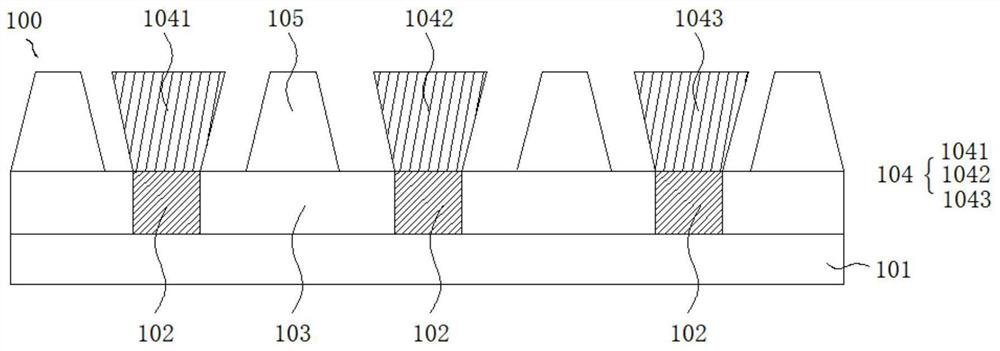
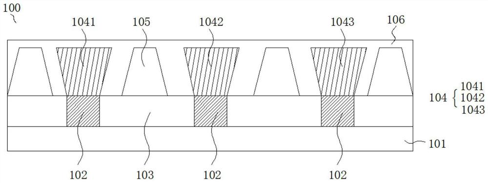
[0045] The preparation method of the display panel in the second embodiment further includes: step S30, preparing a second black matrix flush with the color conversion layer on the array substrate, the second black matrix is ​​located on the near-infrared Micro -In the gap between the LED chip array and the color conversion layer; wherein, the cross-sectional shape of the red conversion layer, blue conversion layer and green conversion layer in the color conversion layer is rectangular, and the cross-sectional shape of the second black matrix It is an upright isosceles trapezoid.

[0046] Figure 10 to Figure 12 It is the concrete preparation method of embodiment two. Such as Figure 10 As shown, the present invention provides an array substrate 101. The array substrate 101 is preferably a thin film transistor substrate. Several near-infrared Micro-LED chips 102 are transferred to the array substrate 101 by a fluid mass transfer method. The surface of the array substrate 101...


PUM


Abstract

The invention provides a display panel and a preparation method thereof. The display panel comprises an array substrate, a near-infrared Micro-LED chip array located on the surface of the array substrate and a color conversion layer located on the surface of the near-infrared Micro-LED chip array. Materials of the color conversion layer comprise a conversion fluorescent material and a rare earth material doped in the conversion fluorescent material, the rare earth material is added to the conversion fluorescent material, and the rare earth material has low phonon energy, so that the non-radiative relaxation probability is greatly reduced, and the luminous efficiency of the conversion fluorescent material is effectively improved. Yb<3+> is serves as a sensitizing agent, Er<3+> serves as an activating agent, and effective near-infrared light-to-visible light up-conversion photoluminescence efficiency can be achieved through energy transfer from the Yb<3+> to the Er<3+>. The Er<3+> and Yb<3+> co-doped up-conversion fluorescent material has the advantages of being high in efficiency and high in color purity, near-infrared light is converted into pure red light, blue light and green light through the color conversion layer, the service life and performance of all near-infrared Micro-LED chips are the same, and a full-color scheme of the Micro-LED is satisfied.

Description

technical field [0001] The present application relates to the field of display technology, in particular, to a display panel and a manufacturing method thereof. Background technique [0002] Micro-Light Emitting Diode (Micro-LED) display is a self-luminous display with Micro-LED chips as pixels. Because of its advantages of high brightness, high luminous efficiency and low power consumption, Micro-LED Relatively speaking, the pixel size is smaller and can be applied to indoor screens and small-size displays. It has gradually become the focus of competition in the international display industry. Many companies in the industry also regard it as the next generation of display technology and begin to actively deploy it. . [0003] Micro-LEDs in the prior art are usually formed by depositing gallium nitride materials on a sapphire substrate. Due to the use of inorganic materials, the current efficiency and lifespan of blue Micro-LEDs are relatively high, but the performance of r...

Claims


Application Information

Patent Timeline
Patent Type & Authority Applications(China)
IPC IPC(8): H01L33/50H01L27/15
CPCH01L33/504H01L33/505H01L27/156H01L2933/0041
Inventor 潘杰
Owner WUHAN CHINA STAR OPTOELECTRONICS SEMICON DISPLAY TECH CO LTD
Why Eureka
Try Eureka