An electrostatic discharge protection semiconductor structure and a method of manufacture

A discharge protection and semiconductor technology, applied in the field of electrostatic discharge protection semiconductor structure, can solve the problems of filament damage, limited usefulness, etc., and achieve the effect of robust electrostatic discharge protection

Pending Publication Date: 2022-01-21
NEXPERIA BV
View PDF0 Cites 0 Cited by
  • Summary
  • Abstract
  • Description
  • Claims
  • Application Information

AI Technical Summary

Problems solved by technology

[0016] These diffusion resistor disadvantages shown by Worley at the 2019 ESD Symposium: Avalanche breakdown combined with snapback at sufficiently high currents
This limits the usefulness of spreading resistors for absorbing the voltage difference between the TVS voltage and the I / O fault voltage
Such diffusion resistors are often damaged by filamentation due to springback

Method used


Image

  • An electrostatic discharge protection semiconductor structure and a method of manufacture
  • An electrostatic discharge protection semiconductor structure and a method of manufacture
  • An electrostatic discharge protection semiconductor structure and a method of manufacture

Examples


Embodiment Construction

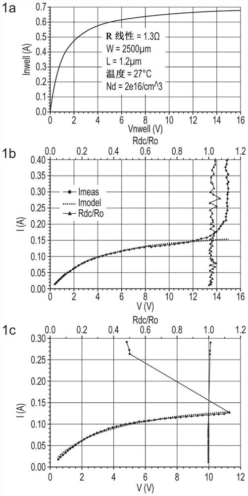
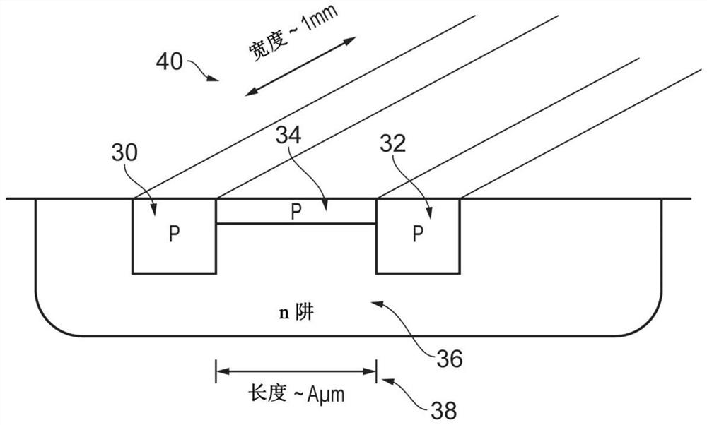
[0046]Embodiments of the present invention relate to velocity-based saturation non-linear resistors having low resistance values ​​for signal transmission current levels and high resistance for ESD current levels. Nonlinear resistors are realized by thin, highly doped diffusions embedded in thicker, similarly highly doped wells with different doping.

[0047] The diffusion resistors according to the invention have no spring back. The resistor will be robust to high current densities since no filamentation will occur. This is achieved with resistors formed from short, thin, highly doped layers embedded in wells with comparable doping levels but with different polarities.

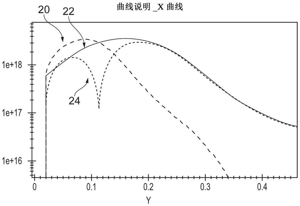
[0048] According to an embodiment of the invention, a suitable implant is used to form a very thin diffusion layer in the range of 0.1 μm with 18 Relatively high doping levels in the range. The corresponding resistive layer is sandwiched between the oxide-covered silicon surface and a similarly highly dope...


PUM

PropertyMeasurementUnit
lengthaaaaaaaaaa
widthaaaaaaaaaa
thicknessaaaaaaaaaa

Abstract

This disclosure relates to a discharge protection semiconductor structure comprising a substrate, a well-positioned on the substrate, a first contact diffusion and a second contact diffusion, the first contact diffusion and the second contact diffusion positioned on the top side of the well, a resistor positioned between the first contact diffusion and a second contact diffusion.

Description

technical field [0001] The invention relates to an electrostatic discharge protection semiconductor structure and a method for forming the electrostatic discharge protection semiconductor structure. The invention also relates to an integrated circuit comprising an electrostatic discharge protected semiconductor structure. Background technique [0002] It is well known that high-speed data transmission integrated circuits are susceptible to electrostatic discharge (ESD) events. Due to the limitation of parasitic line capacitance, the internal protection structure must be small. Additionally, due to the advanced semiconductors required to handle high data rates, the maximum clamping voltage and maximum allowable current are small. [0003] When using external on-board protection, the stress current is shared between the internal protection that is part of the integrated circuit and the external protection device. The greater the impedance in the internal path, the more robu...

Claims


Application Information

Patent Timeline
Patent Type & Authority Applications(China)
IPC IPC(8): H01L27/02H01L21/822
CPCH01L27/0288H01L27/0259H01L27/0296H01L21/822H01L28/20
Inventor 汉斯-马丁·里特
Owner NEXPERIA BV
Why Eureka
Try Eureka