Display panel

A display panel and sub-pixel technology, applied in the manufacturing of electrical components, electrical solid-state devices, semiconductor/solid-state devices, etc., can solve the problems of packaging failure, color mixing, easy scratching of metal masks, etc., to improve yield and reduce design. Difficulty, the effect of reducing the risk of being scratched

Pending Publication Date: 2022-01-11
WUHAN CHINA STAR OPTOELECTRONICS SEMICON DISPLAY TECH CO LTD
View PDF0 Cites 0 Cited by
  • Summary
  • Abstract
  • Description
  • Claims
  • Application Information

AI Technical Summary

Problems solved by technology

[0004] The purpose of the present invention is to provide a display panel to solve the technical problems of color mixing in adjacent sub-pixels in the pixel structure obtained by evaporation in the prior art, and the metal mask plate is easy to scratch the spacer column layer, resulting in package failure.

Method used


Image

  • Display panel
  • Display panel
  • Display panel

Examples


Embodiment 1

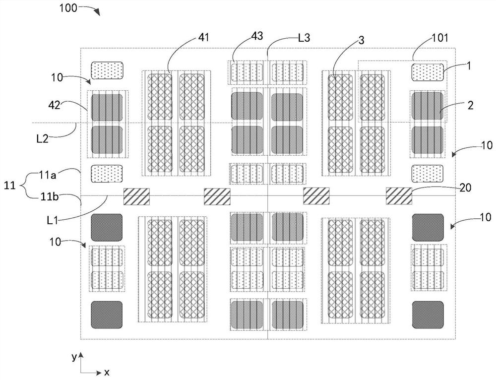
[0040] This embodiment provides a display panel, which is an OLED display panel, and includes a pixel structure 100 in which a plurality of sub-pixels are arranged.

[0041] Such as figure 1 As shown, this embodiment provides a pixel structure 100, including a plurality of pixel unit groups 10 arranged in an array, and the sub-pixels in each pixel unit group 10 are arranged according to a preset virtual pattern, and the virtual pattern includes Two virtual rectangles 11 adjacently arranged according to the first direction y. Wherein, the two pixel unit groups 10 arranged adjacently along the first direction y (that is, the two adjacently arranged pixel unit groups 10 arranged up and down) are a minimum repeating unit, that is, a matrix of 8 rows and 4 columns arranged sub-pixels.

[0042] Each pixel unit group 10 is four pixel units 101 arranged in a matrix, and each pixel unit 101 includes a first sub-pixel 1, a second sub-pixel 2 and a third sub-pixel 3, wherein the first ...

Embodiment 2

[0057] This embodiment provides a display panel, which includes most of the features of Embodiment 1, the difference being that in the same pixel unit group 10, the second sub-pixels of more than two pixel units 101 arranged along the first direction y 2. The third sub-pixels 3 are arranged on the same line and arranged alternately; a plurality of spacer columns 20 are arranged at intervals at the midpoint of the first boundary line L1.

[0058] Such as image 3 As shown, this embodiment provides a pixel structure 200, including a plurality of pixel unit groups 10 arranged in an array, and the sub-pixels in each pixel unit group 10 are arranged according to a preset virtual pattern, and the virtual pattern includes Two virtual rectangles 11 adjacently arranged according to the first direction y. Wherein, the two pixel unit groups 10 arranged adjacently along the first direction y (that is, the two adjacently arranged pixel unit groups 10 arranged up and down) are a minimum re...


PUM


Abstract

The invention discloses a display panel, which comprises a pixel structure. The pixel structure comprises a plurality of pixel unit groups, sub-pixels in each pixel unit group are arranged according to a preset virtual graph, and the virtual graph comprises two virtual rectangles which are adjacently arranged according to a first direction. Each pixel unit group comprises a plurality of sub-pixels with different colors, the first sub-pixel is arranged close to the central point of the virtual rectangle, and the second sub-pixel and the third sub-pixel are arranged in the virtual graph in the first direction and are arranged close to the two side edges; and the area of the first sub-pixel is larger than that of the second sub-pixel or that of the third pixel. Each first sub-pixel comprises a first electrode, a first light-emitting layer and a second electrode which are sequentially stacked, and in the same pixel unit group, the first light-emitting layer covers at least two adjacent first electrodes so as to merge the evaporation openings, so that the design difficulty of the mask plate and the color mixing risk after evaporation are reduced.

Description

technical field [0001] The present application relates to the field of display technology, and in particular to a display panel. Background technique [0002] The 21st century is called a brand-new "electronic information age". The development of the network has increased people's demand for information. Smart phones, watches, and (tablet) computers have become an indispensable part of people's lives. The advent of the information age has greatly promoted the development of display technology. People's pursuit of thinner and more energy-saving large-size and flexible display devices has made organic electroluminescence become the mainstream of the market. [0003] OLED (Organic Light Emitting Diode, Organic Light Emitting Diode) has the characteristics of self-luminescence, fast response speed, wide viewing angle, etc., and has broad application prospects. At present, all OLED devices use a fine metal mask (Fine Metal Mask, FMM) to realize evaporation of RGB light-emitting ...

Claims


Application Information

Patent Timeline
IPC IPC(8): H01L51/50H01L51/52H01L27/32
CPCH10K59/352H10K59/353H10K50/11H10K2101/10H10K50/8428
Inventor 王芳
Owner WUHAN CHINA STAR OPTOELECTRONICS SEMICON DISPLAY TECH CO LTD
Why Eureka
Try Eureka