Semiconductor device assemblies and systems with improved thermal performance and methods for making the same

A technology of semiconductors and assemblies, applied in semiconductor/solid-state device manufacturing, semiconductor devices, semiconductor/solid-state device components, etc.

Pending Publication Date: 2021-12-24
MICRON TECH INC
View PDF0 Cites 0 Cited by
  • Summary
  • Abstract
  • Description
  • Claims
  • Application Information

AI Technical Summary

Problems solved by technology

During operation, semiconductor die can generate heat, which can challeng

Method used


Image

  • Semiconductor device assemblies and systems with improved thermal performance and methods for making the same
  • Semiconductor device assemblies and systems with improved thermal performance and methods for making the same
  • Semiconductor device assemblies and systems with improved thermal performance and methods for making the same

Examples


Embodiment Construction

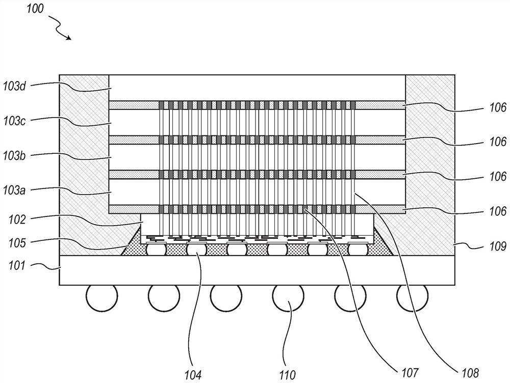
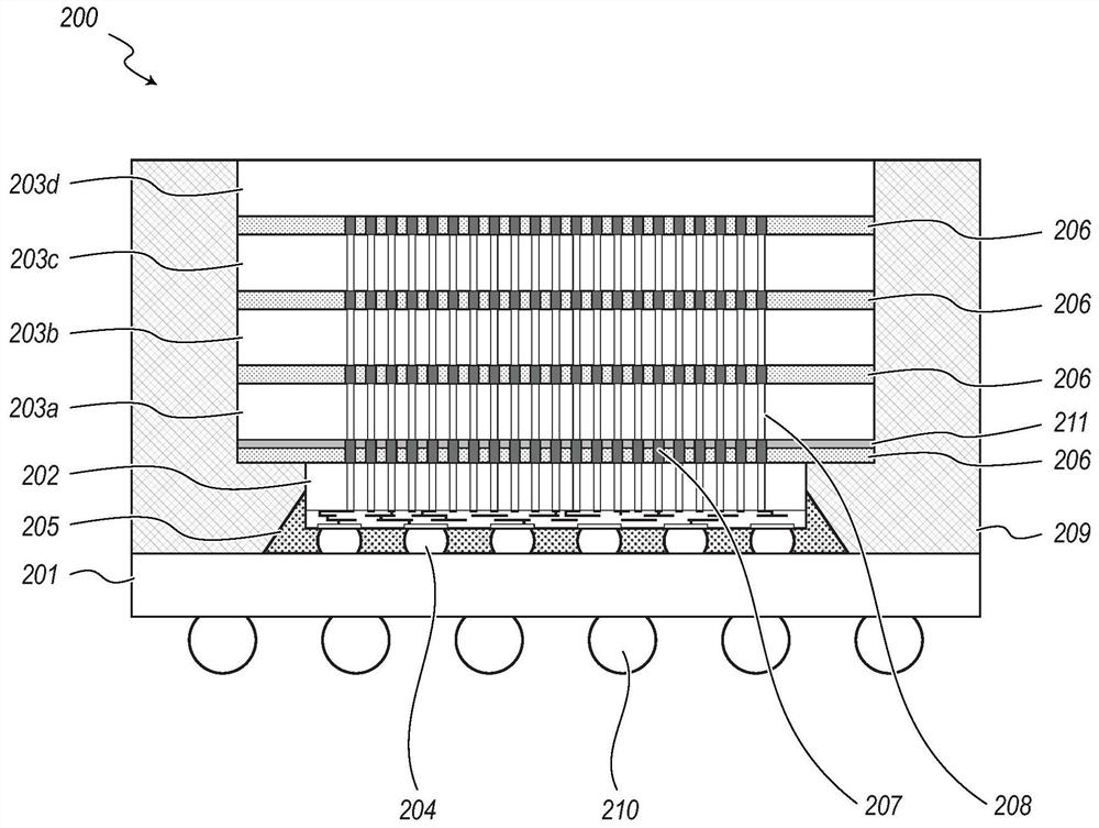
[0015] Certain details of several embodiments of semiconductor devices and related systems and methods are described below. Those of ordinary skill in the relevant art will recognize that suitable stages of the methods described herein may be performed at the wafer level or at the die level. Thus, depending on the context of its use, the term "substrate" may refer to a wafer-level substrate or a singulated die-level substrate. In addition, unless the context dictates otherwise, conventional semiconductor fabrication techniques may be used to form the structures disclosed herein. Materials may be deposited, for example, using chemical vapor deposition, physical vapor deposition, atomic layer deposition, electroplating, electroless plating, spin coating, and / or other suitable techniques. Similarly, material may be removed, for example, using plasma etching, wet etching, chemical mechanical planarization, or other suitable techniques.

[0016] figure 1 is a simplified schemat...


PUM

PropertyMeasurementUnit
Thicknessaaaaaaaaaa

Abstract

The invention relates to semiconductor device assemblies and systems with improved thermal performance and methods for making the same. Semiconductor device assemblies are provided with one or more layers of thermally conductive material disposed between adjacent semiconductor dies in a vertical stack. The thermally conductive material can be configured to conduct heat generated by one or more of the semiconductor dies in laterally outward towards an outer edge of the assembly. The layer of thermally conductive material can comprise one or more allotropes of carbon, such as diamond, graphene, graphite, carbon nanotubes, or a combination thereof. The layer of thermally conductive material can be provided via deposition (e.g., sputtering, PVD, CVD, or ALD), or via adhering a film comprising the layer of thermally conductive material to one or more of the semiconductor dies.

Description

[0001] Cross References to Related Applications [0002] This application claims the benefit of U.S. Provisional Patent Application No. 63 / 043,685, filed June 24, 2020, which is hereby incorporated by reference in its entirety. technical field [0003] The present disclosure relates generally to semiconductor devices, and more particularly, to semiconductor device assemblies and systems with improved thermal performance and methods of making the same. Background technique [0004] Packaged semiconductor die, including memory chips, microprocessor chips, and imager chips, typically include one or more semiconductor die mounted on a substrate and enclosed in a protective covering or capped with a thermally conductive cover. In operation, semiconductor die can generate heat, which can challenge package design as the number of devices and their power densities increase. Various methods of managing the heat generated include providing a heat dissipation structure, such as a lid...

Claims


Application Information

Patent Timeline
IPC IPC(8): H01L23/367H01L23/373H01L21/50H01L21/56
CPCH01L23/367H01L23/3738H01L23/373H01L21/50H01L21/56H01L23/3732H01L23/3672H01L23/49816H01L23/3128H01L25/0657H01L25/50H01L2225/06589H01L24/10H01L2224/32145H01L2224/16225H01L2224/16145H01L2224/16146H01L2224/73204H01L2924/181H01L2224/32225H01L2924/15311H01L2924/18161H01L24/16H01L2924/00012H01L2924/00
Inventor 全炫锡曲小鹏
Owner MICRON TECH INC
Why Eureka
Try Eureka