Refrigeration packaging structure of electro-absorption modulated laser

A technology of electro-absorption modulation and packaging structure, used in lasers, laser parts, semiconductor lasers, etc., can solve problems such as long distance, affecting the cooling effect of semiconductor refrigerators, and long gold wire length, ensuring signal transmission and avoiding refrigeration. effect, effect of reducing the number of

Active Publication Date: 2021-12-07
武汉敏芯半导体股份有限公司
View PDF13 Cites 0 Cited by
  • Summary
  • Abstract
  • Description
  • Claims
  • Application Information

AI Technical Summary

Problems solved by technology

[0004] The electro-absorption modulation laser chip is connected to the pins of the base through gold wires. Since the distance between the pins and the electro-absorption modulation laser chip is usually relatively long, the length of the gold wire is relatively long. Moreover, the connection between the electro-absorption modulation laser chip and the pins The number of gold wires is usually large, which causes more heat to be conducted by the gold wires into the package, thereby affecting the cooling effect of the semiconductor cooler on the electroabsorption modulation laser

Method used


Image

  • Refrigeration packaging structure of electro-absorption modulated laser
  • Refrigeration packaging structure of electro-absorption modulated laser
  • Refrigeration packaging structure of electro-absorption modulated laser

Examples


Embodiment Construction

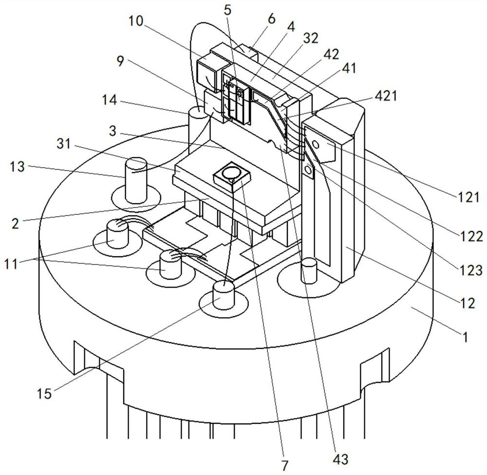
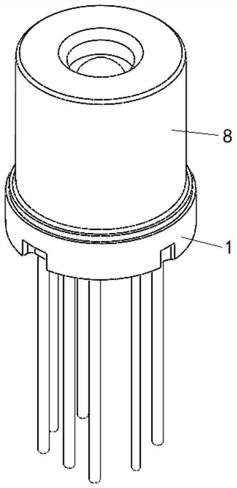
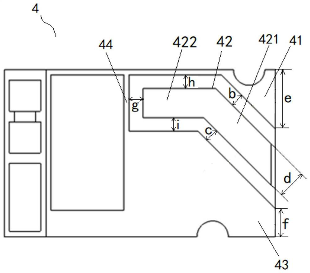
[0038] In order to make the purpose, technical solutions and advantages of the present invention clearer, the technical solutions in the embodiments of the present invention will be described in more detail below with reference to the drawings in the preferred embodiments of the present invention. In the drawings, the same or similar reference numerals denote the same or similar elements or elements having the same or similar functions throughout. The described embodiments are some, but not all, embodiments of the invention. The embodiments described below by referring to the figures are exemplary and are intended to explain the present invention and should not be construed as limiting the present invention. Based on the embodiments of the present invention, all other embodiments obtained by persons of ordinary skill in the art without creative efforts fall within the protection scope of the present invention. Embodiments of the present invention will be described in detail b...


PUM

PropertyMeasurementUnit
thicknessaaaaaaaaaa

Abstract

The invention discloses a refrigeration packaging structure of an electro-absorption modulated laser, relates to the technical field of chip packaging, and mainly aims to ensure that the impedance of a signal wire and a ground wire of an electro-absorption modulated laser is 48-52 ohms and prevent the refrigeration effect of a semiconductor refrigerator from being influenced by heat conduction of a gold wire. The packaging structure comprises: a base; a semiconductor cooler arranged on the base; an L-shaped tungsten copper block, wherein the horizontal end of the L-shaped tungsten copper block is arranged on the semiconductor cooler; a carrier plate, wherein the carrier plate is arranged at the vertical end, the first routing end of a first signal pin of the carrier plate is horizontally opposite to the routing end of a second signal pin of the carrier plate through two gold threads, the first ground pin is horizontally opposite to the third ground pin through two gold threads, and the second ground pin is horizontally opposite to the fourth ground pin through two gold threads; an electro-absorption modulated laser chip, wherein the electro-absorption modulated laser chip is arranged on the carrier plate, one end of the electro-absorption modulated laser chip is connected with the first signal pin, and the other end of the electro-absorption modulated laser chip is connected with the third pin; a thermistor arranged at the vertical end; a backlight monitoring detector chip arranged at the horizontal end; and a lens cap packaged on the base.

Description

technical field [0001] The invention relates to the technical field of chip packaging, in particular to a refrigeration packaging structure for an electroabsorption modulation laser. Background technique [0002] Electroabsorption modulated lasers are integrated devices of distributed feedback lasers and electroabsorption modulators, and are usually widely used as key signal light sources in long-distance communication trunk lines and high-speed optical fiber transmission systems. [0003] At present, the electro-absorption modulation laser can adopt a TO cooling package structure, which usually includes a semiconductor cooler, and the semiconductor cooler is used to control the temperature of the electro-absorption modulation laser to ensure the operating temperature of the electro-absorption modulation laser. [0004] The electro-absorption modulation laser chip is connected to the pins of the base through gold wires. Since the distance between the pins and the electro-abs...

Claims


Application Information

Patent Timeline
Patent Type & Authority Applications(China)
IPC IPC(8): H01S5/02212H01S5/0232H01S5/02345H01S5/0237H01S5/024H01S5/026
CPCH01S5/0232H01S5/02345H01S5/0261H01S5/02212H01S5/0237H01S5/02415
Inventor 刘永康刘倚红王任凡
Owner 武汉敏芯半导体股份有限公司
Why Eureka
Try Eureka