Display device with destaticizing element

A display device and anti-static technology, which can be used in identification devices, nonlinear optics, instruments, etc., and can solve the problem of not fully protecting transistors or insulating films.

Inactive Publication Date: 2004-02-04
CASIO COMPUTER CO LTD
View PDF0 Cites 0 Cited by
  • Summary
  • Abstract
  • Description
  • Claims
  • Application Information

AI Technical Summary

Problems solved by technology

In this way, the antistatic element 9 cannot completely protect the transistor or the insulating film.

Method used


Image

  • Display device with destaticizing element
  • Display device with destaticizing element
  • Display device with destaticizing element

Examples


no. 1 example

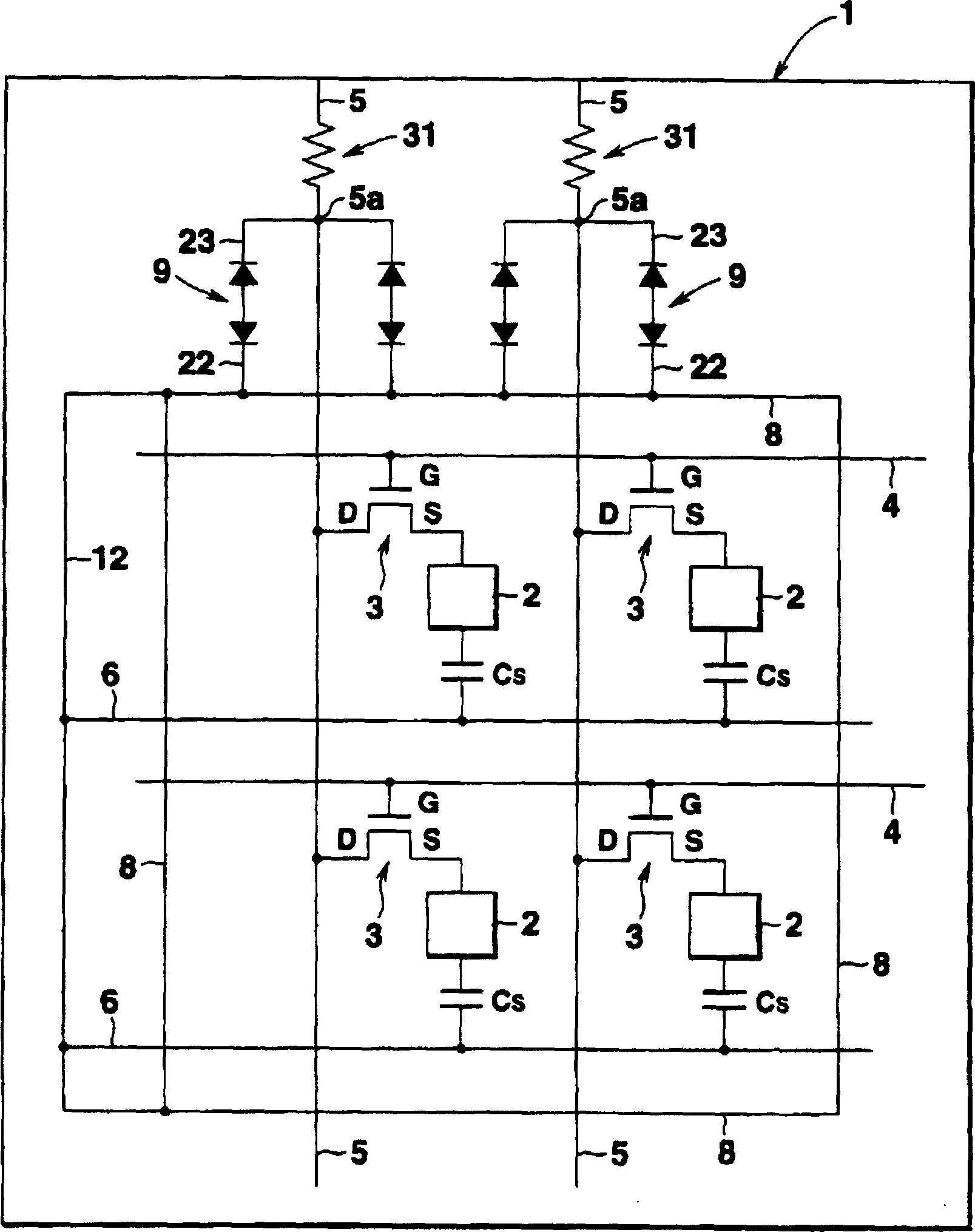
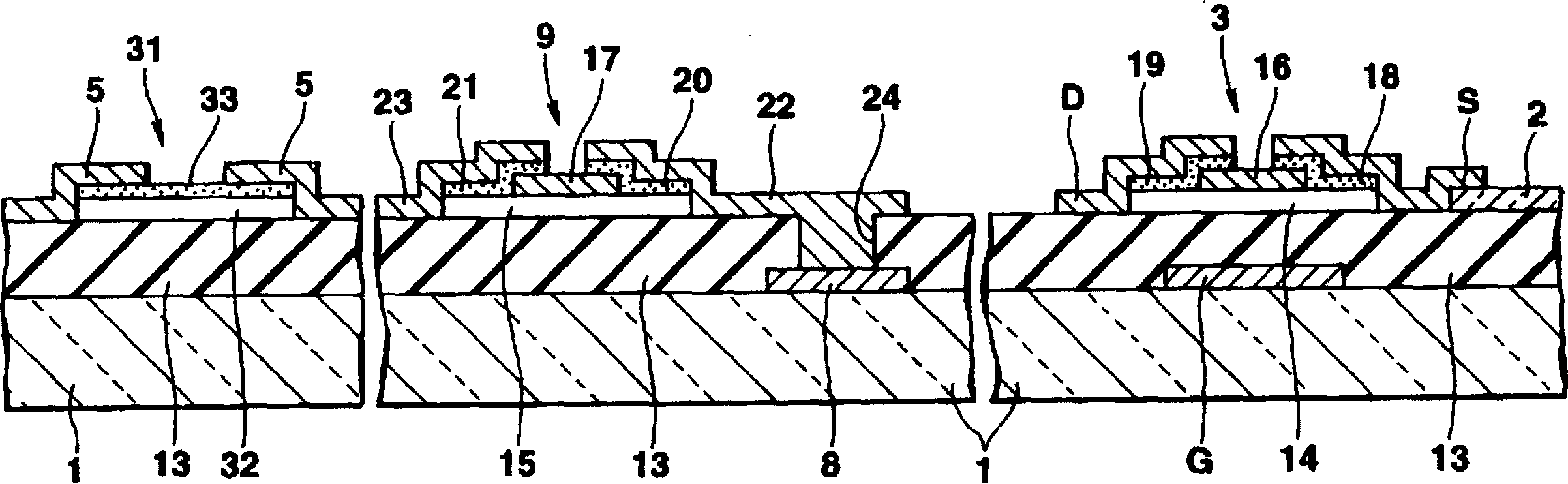
[0037] figure 1 It is a diagram of the circuit scheme on the active element substrate in the liquid crystal display device according to the first embodiment of the present invention. figure 2 yes figure 1 The enlarged cross-sectional view of the active element substrate in the middle part. Such as figure 1 with figure 2 As shown, the gate G of the thin film transistor 3 is fabricated on the active element substrate 1 . especially if Figure 9 As shown, the scanning line 4, the auxiliary capacitor line 6, the upper and lower sides of the common line 12 and the short-circuit line 8, and the gate G are fabricated on the active element substrate 1 at the same time.

[0038] A gate insulating film 13 including the gate G is formed on the entire surface of the active element substrate 1, and a semiconductor thin film 14 made of pure amorphous silicon is formed on the gate insulating film 13 in phase with each gate G. in the corresponding area. Similarly, a semiconductor ...


PUM


Abstract

A pair of destaticizing elements and a resistive element for delaying an electrostatic pulse are provided between a short-circuiting line short-circuiting a plurality of data lines and an upper end portion of each of the data lines. When a short electrostatic pulse is applied to an upper end portion of one data line from the outside, the leading edge of the pulse is made gentle by the resistive element. As a result, the destaticizing element can work well in response to even the short electrostatic pulse.

Description

technical field [0001] The present invention relates to a display device, in particular to an active matrix liquid crystal display device with a semiconductor element, which includes a destaticizing element for protecting the semiconductor element and insulating film from electrostatic breakdown. Background technique [0002] Figure 10 It is a schematic diagram of the circuit on the active element substrate in a general liquid crystal display device. A plurality of pixel electrodes (not shown) constituting a display area and a thin film transistor connected to a corresponding one of the pixel electrodes are arranged in a matrix on the active element substrate 1 . On the active element substrate 1 there are multiple scanning lines 4 , multiple data lines 5 , multiple auxiliary capacitor lines 6 , multiple input lines 7 , a circular short circuit 8 and multiple destaticizing elements 9 . Among them, the scanning line 4 is used to provide the scanning signal to the correspond...

Claims


Application Information

Patent Timeline
IPC IPC(8): G09F9/00G02F1/1345G02F1/1362
CPCG02F1/136204G02F1/1345G02F1/136286G02F2202/22
Inventor 日置利文宫田敬太郎
Owner CASIO COMPUTER CO LTD
Why Eureka
Try Eureka