Device for clamping silicon wafer in silicon wafer visual detection process

A technology for visual detection and silicon wafers, which is applied in the direction of workpiece clamping devices, manufacturing tools, workbenches, etc., can solve problems such as the inability to realize silicon wafer detection and blind spots caused by visual inspection, and achieve good protection, convenient inspection, and prevention of silicon wafers. The effect of chip damage

Pending Publication Date: 2021-11-30
扬州晶樱光电科技有限公司
View PDF6 Cites 0 Cited by
  • Summary
  • Abstract
  • Description
  • Claims
  • Application Information

AI Technical Summary

Problems solved by technology

[0005] The object of the present invention is to provide a device for clamping silicon wafers in the process of visual inspection of silicon wafers, so as to solve the problem of clamping the corners of silicon wafers proposed in the above background technology, which will cause blind spots in visual inspection and cannot be realized. The problem of all-round detection of silicon wafers

Method used


Image

  • Device for clamping silicon wafer in silicon wafer visual detection process
  • Device for clamping silicon wafer in silicon wafer visual detection process
  • Device for clamping silicon wafer in silicon wafer visual detection process

Examples


Embodiment

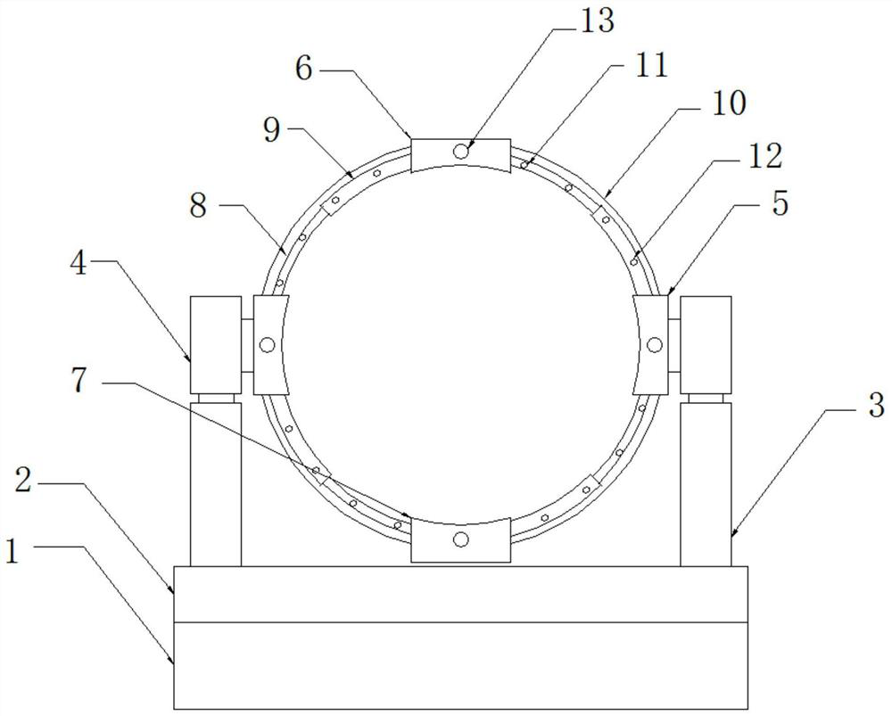
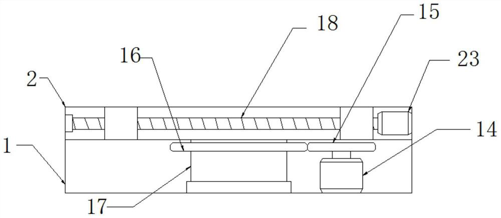
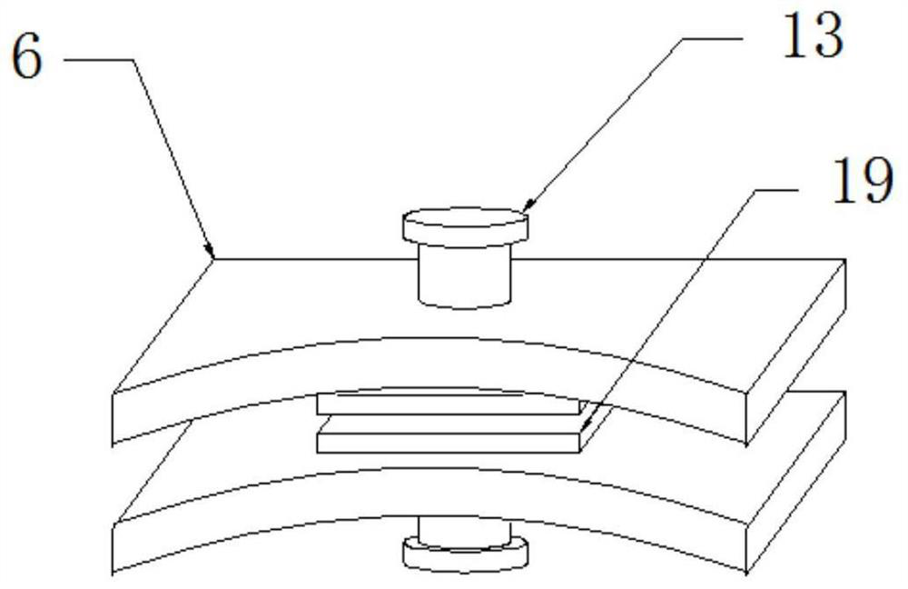
[0026] see Figure 1-5 , the present invention provides a technical solution: a device for clamping silicon wafers in the process of visual inspection of silicon wafers, including a turntable 2, an adjustment column 3, a mounting seat 4 and a clamping mechanism, and the turntable 2 is equipped with There is a driving mechanism for adjusting the position of the adjusting column 3, the driving mechanism can drive the displacement of the adjusting column 3, and the adjusting column 3 is provided with a hydraulic device, the telescopic end of the hydraulic device runs through the adjusting column 3 and is connected with the mounting seat 4, the hydraulic device The work can drive the mounting seat 4 to rise or fall. The clamping mechanism includes two fixed seats 6, two left and right connecting seats 5, a driving seat 7 and a connecting mechanism. Connected to the seat 4, the mounting seat 4 is provided with a connecting block, the bearing is connected to the connecting block, an...


PUM


Abstract

The invention belongs to the technical field of silicon wafer production, and particularly relates to a device for clamping a silicon wafer in a silicon wafer visual detection process. The device comprises a rotary disc, adjusting columns, mounting seats and a clamping mechanism, wherein a driving mechanism for adjusting the positions of the adjusting columns is arranged in the rotary disc, hydraulic devices are arranged in the adjusting columns, the telescopic ends of the hydraulic devices penetrate through the adjusting columns and are connected with the mounting seats, the clamping mechanism comprises two fixing seats, a left connecting seat, a right connecting seat, a driving seat and a connecting mechanism, and the left connecting seat and the right connecting seat are connected with the mounting seats close to the left connecting seat and the right connecting seat through bearings respectively. According to the device, the silicon wafer can penetrate through the space between the two fixing seats to be inserted into grooves in the driving seat and the connecting seats, and the connecting seats are rotated to drive the silicon wafer to rotate so that the surface of the silicon wafer can be observed; and meanwhile, a first motor can drive rubber driving rollers to rotate so as to drive the silicon wafer to rotate so that the corners of the silicon wafer can be conveniently inspected visually, and all-directional inspection of the silicon wafer is realized.

Description

technical field [0001] The invention relates to the technical field of silicon wafer production, in particular to a device for clamping silicon wafers during the visual inspection process of silicon wafers. Background technique [0002] With the rapid development of the information age, the society's demand for electronic chips is increasing rapidly. At the same time, people's requirements for the quality of silicon wafers, the raw material for making chips, are also getting higher and higher. [0003] During the manufacturing process of silicon wafers, defects may occur on silicon wafers, including edge chipping, scratches, cracks, etc. These defects will bring great risks to further downstream production and utilization. Therefore, all-round inspection of silicon wafers inspection is crucial. Visual inspection is an important defect detection method. This method refers to irradiating the light beam generated by the strong light onto the surface of the silicon wafer, and a...

Claims


Application Information

Patent Timeline
IPC IPC(8): B25B11/00B25H1/10
CPCB25B11/00B25H1/10
Inventor 杨定勇朱庆龙张力峰
Owner 扬州晶樱光电科技有限公司
Why Eureka
Try Eureka