Appearance leveling device for PCB

A technology of PCB circuit board and leveling device, which is applied in the direction of secondary processing of printed circuits, etc., can solve the problems of tin copper slag falling into tin pool, and the inability of flux to be discharged.

Active Publication Date: 2021-11-26
南通华钛电子科技有限公司
View PDF4 Cites 0 Cited by
  • Summary
  • Abstract
  • Description
  • Claims
  • Application Information

AI Technical Summary

Problems solved by technology

[0007] The purpose of the present invention is to provide a device for leveling the appearance of PCB circuit boards, so as to solve the technical problem in the prior art that the tin-copper slag falls into the tin pool and the flux cannot be discharged

Method used


Image

  • Appearance leveling device for PCB
  • Appearance leveling device for PCB
  • Appearance leveling device for PCB

Examples


Embodiment Construction

[0034] The following will clearly and completely describe the technical solutions in the embodiments of the present invention with reference to the accompanying drawings in the embodiments of the present invention. Obviously, the described embodiments are only some, not all, embodiments of the present invention. Based on the embodiments of the present invention, all other embodiments obtained by persons of ordinary skill in the art without making creative efforts belong to the protection scope of the present invention.

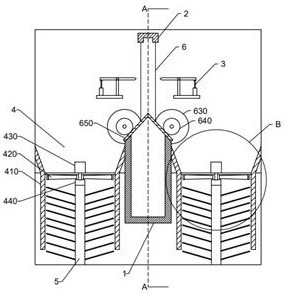
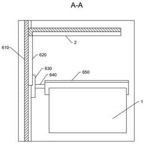
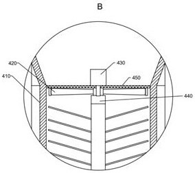
[0035] Such as Figure 1 to Figure 6 As shown, the present invention provides a profile leveling device for a PCB circuit board, comprising a tin pool 1, a fixture 2, an air knife assembly 3 and an air suction assembly 4, the tin pool 1 is used to hold metal tin melt, and The upper end is provided with an opening, and the fixture 2 is used to clamp the PCB circuit board. The fixture 2 is arranged above the opening and reciprocates in the vertical direction. C...


PUM


Abstract

The invention discloses an appearance leveling device for a PCB; the device comprises a tin pool, a clamp, an air knife assembly and an air suction assembly, the tin pool is used for containing metal tin melt, an opening is formed in the upper end of the tin pool, the clamp is arranged above the opening and reciprocates in the vertical direction, the air suction assembly is provided with an air suction opening, and blades are rotationally arranged in the air suction opening. After the blades rotate, hot air is extracted, tin-copper slag and volatilized scaling powder are sucked, a condensation piece is further arranged in the air suction opening, and the condensation piece adsorbs the scaling powder and separates out the tin-copper slag. The air suction assembly is arranged, tin-copper slag blown off by an air knife is collected through strong wind power while heat dissipation is conducted, the tin-copper slag is prevented from falling into a tin pool, and the influence of metal copper on the tin pool is effectively avoided; meanwhile, after the hot air passes through the condensation piece, the scaling powder can be rapidly cooled and separated out, and the scaling powder is prevented from being attached to all parts of the device and corroding important parts.

Description

technical field [0001] The invention relates to the technical field of PCB circuit board processing, in particular to a shape leveling device for a PCB circuit board. Background technique [0002] PCB (Printed Circuit Board) circuit board, the Chinese name is printed circuit board, also known as printed circuit board, is an important electronic component, a support for electronic components, and a carrier for electrical interconnection of electronic components. [0003] The printed circuit board is composed of an insulating base plate, connecting wires and pads for assembling and welding electronic components, and has the dual functions of a conductive line and an insulating base plate. It can replace complex wiring and realize the electrical connection between components in the circuit, which not only simplifies the assembly and welding of electronic products, reduces the workload of wiring in traditional methods, and greatly reduces the labor intensity of workers; it also ...

Claims


Application Information

Patent Timeline
Patent Type & Authority Applications(China)
IPC IPC(8): H05K3/22
CPCH05K3/22
Inventor 彭海军
Owner 南通华钛电子科技有限公司
Why Eureka
Try Eureka