
Encrypted data reading and writing method of spi storage device and embedded processor chip

A technology for storage devices and encrypted data, applied in the protection of internal/peripheral computer components, etc., can solve problems such as missing online encrypted writing, feature mismatch, unfriendly SPINAND support, etc., to achieve real-time completion without affecting the transmission rate Effect

Active Publication Date: 2022-02-22
广州匠芯创科技有限公司
View PDF0 Cites 0 Cited by
  • Summary
  • Abstract
  • Description
  • Claims
  • Application Information

AI Technical Summary

Problems solved by technology

There are two reasons here. One is that the decryption unit and the bus transmission are designed to be serial; the other is that the choice of encryption algorithm also has an impact. Some algorithms must wait for enough data to arrive before they can be decrypted.
[0008] The second disadvantage is that the support for SPI NAND is not friendly
The current scheme maps the encrypted data area through Cache, and Cache can be read randomly, but SPINAND cannot be read randomly.
Due to the mismatch of the characteristics of the two devices, the SPI NAND device cannot be well supported
[0009] The third disadvantage is that it is not friendly to write operation support
For this reason, the current technical solutions usually only see the function of online decryption and reading, but not the function of online encryption and writing

Method used


Image

  • Encrypted data reading and writing method of spi storage device and embedded processor chip
  • Encrypted data reading and writing method of spi storage device and embedded processor chip
  • Encrypted data reading and writing method of spi storage device and embedded processor chip

Examples


Embodiment Construction

[0034] Embodiments of the present invention are described in detail below, examples of which are shown in the drawings, wherein the same or similar reference numerals designate the same or similar elements or elements having the same or similar functions throughout. The embodiments described below by referring to the figures are exemplary only for explaining the present invention and should not be construed as limiting the present invention.

[0035] In the description of the present invention, the meaning of several means one or more, and the meaning of multiple means two or more than two. Greater than, less than, exceeding, etc. are understood as not including the original number, and above, below, within, etc. are understood as including the original number . If the description of the first and second is only for the purpose of distinguishing the technical features, it cannot be understood as indicating or implying the relative importance or implicitly indicating the number...


PUM


Abstract

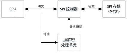
The embodiment of the present invention discloses a method for reading and writing encrypted data of an SPI storage device and an embedded processor chip, wherein the method for reading encrypted data includes: setting the address of the data to be accessed to an encryption and decryption processing unit in response to the CPU, and the encryption and decryption processing The unit calculates the grouping key according to the data address to be accessed; the SPI controller initiates data access and transmission operations to the SPI storage device according to the data address to be accessed; the SPI controller reads the corresponding grouping key from the encryption and decryption unit key, performing an XOR operation on the group key and the ciphertext data received from the SPI storage device to obtain decrypted data; the CPU receives the decrypted data from the SPI controller. The embodiment of the present invention implements online encryption for data writing and online decryption for reading; the encryption and decryption process of data is completed in real time, and the reading and writing rate is not affected.

Description

technical field [0001] The invention relates to the technical field of electronic chips, in particular to a method for reading and writing encrypted data of an SPI storage device and an embedded processor chip. Background technique [0002] SPI storage devices refer to storage devices that use the SPI bus interface, such as SPI NOR, SPI NAND, and SPI SRAM. Generally, SPI storage devices have small capacity and relatively low cost, and are commonly used in embedded devices. [0003] The online encrypted storage of the SPI storage device refers to a technology in which the data stored on the storage device is encrypted data, but the data read by the CPU is plaintext data. Using this technology, the data stored on the SPI storage device can be encrypted and protected, and the encryption process can be hidden and transparent to the CPU, so that users can use it more easily. [0004] refer to figure 1 , the implementation process of the online encrypted storage technology of t...

Claims


Application Information

Patent Timeline
Patent Type & Authority Patents(China)
IPC IPC(8): G06F21/79
CPCG06F21/79
Inventor 吴德煌原顺
Owner 广州匠芯创科技有限公司
Learn More