
Sensing, storing and calculating integrated circuit structure for realizing positive and negative weight calculation in pixels

A circuit structure and pixel circuit technology, applied in TV, electrical components, image communication, etc., can solve the problems of low operation speed, high power consumption, low circuit integration, etc., and achieve the effect of reducing power consumption and cost, and saving area.

Active Publication Date: 2021-11-02
UNIV OF ELECTRONIC SCI & TECH OF CHINA
View PDF6 Cites 2 Cited by
  • Summary
  • Abstract
  • Description
  • Claims
  • Application Information

AI Technical Summary

Problems solved by technology

[0005] At present, although the existing integrated storage and computing technology has been relatively mature; however, the CMOS image sensor chip, the computing unit, and the storage unit are independent circuit modules. This von Neumann structure leads to low computing speed and relatively high High power consumption and low circuit integration

Method used


Image

  • Sensing, storing and calculating integrated circuit structure for realizing positive and negative weight calculation in pixels
  • Sensing, storing and calculating integrated circuit structure for realizing positive and negative weight calculation in pixels
  • Sensing, storing and calculating integrated circuit structure for realizing positive and negative weight calculation in pixels

Examples


Embodiment Construction

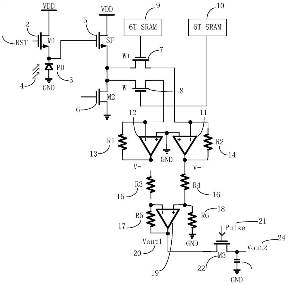
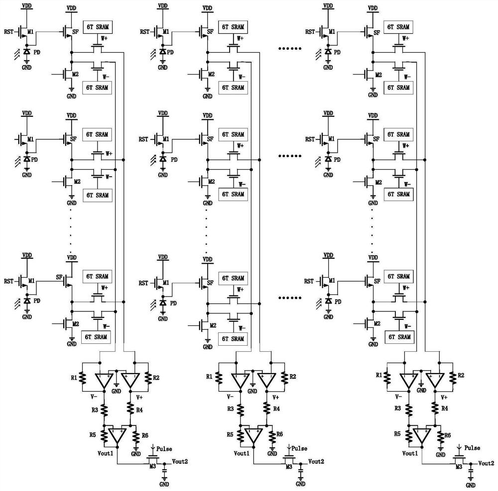
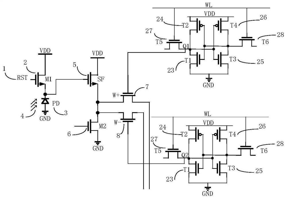
[0035]When researching the existing CMOS image sensor sensing, storage and computing circuits, it is found that the active pixels of the CMOS image sensor exist in the form of a large-scale pixel array, that is, the pixel array, storage unit, and computing unit are all independent circuit modules. This von Neumann structure will result in a large area, low computing speed, and high power consumption. By adopting the idea of ​​integrating image sensing technology, data storage technology and data computing technology, and combining CMOS active pixel circuit with 6TSRAM memory and operational amplifier circuit, data sensing can be realized in one pixel unit , storage and linear operation, so as to achieve the purpose of saving storage area, reducing computing power consumption and improving computing speed. On the basis of the prior art, the present invention proposes a sensor-storage-calculation integrated circuit structure based on realizing positive and negative weight calcul...


PUM


Abstract

The invention belongs to the technical field of image sensing and integrated circuits, and particularly relates to a sensing, storing and calculating integrated circuit structure for realizing positive and negative weight calculation in pixels. According to the circuit, a positive and negative weight selection unit module is used for shunting induced current generated by a CMOS active pixel unit module during illumination, then a summing and differencing operation circuit module is used for operating and converting the current, and finally a voltage sampling circuit module is used for periodically sampling voltage signals. Compared with a traditional in-memory calculation circuit, the sensing, storing and calculating integrated circuit structure for realizing the positive and negative weight operation based on the pixels utilizes a CMOS active pixel structure to realize sensing, uses a positive and negative weight selection tube and a 6T SRAM as storage and an operational amplifier as a calculation unit, and integrates sensing and in-memory calculation, the sensing data calculation speed of the circuit can be greatly improved, the integration level is high, the structure is simple, and the power consumption is low.

Description

technical field [0001] The invention belongs to the field of image sensing technology and integrated circuit technology, and in particular relates to a sensor-storage-calculation integrated circuit structure based on realizing positive and negative weight calculations in pixels. Background technique [0002] The pixel of the CMOS image sensor is an active pixel sensor APS (Active Pixel Sensor). There is a photodiode in each pixel unit as the basic photoelectric conversion element, and each pixel also includes a source follower MOSFET, which is used as a switch. And the reset MOSFET, by applying light intensity to the photodiode, the photosensitive and excited carrier charge signal is converted into a voltage signal, and the exposure operation and signal output of the photodiode are controlled by an analog switch. However, combining the sensing unit with the computing and storage units will have a great impact on the performance of the entire system. Moreover, in the traditi...

Claims


Application Information

Patent Timeline
IPC IPC(8): H04N5/374
CPCH04N25/76
Inventor 胡绍刚张宗镒黄家刘洋于奇
Owner UNIV OF ELECTRONIC SCI & TECH OF CHINA
Learn More