Active grounding circuit and method based on negative feedback loop control

A technology of loop control and grounding circuit, which is applied in the direction of control/regulation system, adjustment of electrical variables, instruments, etc., can solve the problems of reduced accuracy, wrong test results, and poor test performance, so as to suppress zero drift and control simple and reliable , reducing the effect of distortion

Active Publication Date: 2021-10-08
THE 41ST INST OF CHINA ELECTRONICS TECH GRP
View PDF4 Cites 0 Cited by
  • Summary
  • Abstract
  • Description
  • Claims
  • Application Information

AI Technical Summary

Problems solved by technology

The grounding system of traditional test instruments is to connect the ground plane to a fixed level. Due to the resistance of the power supply output line, as the output current changes, the voltage on the line will change, and the level of the grounding system will also change. will change accordingly, which will seriously affect the test accuracy and restrict the development of semiconductor test technology
[0003] Semiconductor test accuracy requirements have reached microvolts or even nanovolts, and weak voltage fluctuations in the grounding system of test instruments will lead to sharp deterioration of test performance, significantly reduced accuracy, and even wrong test results
The traditional grounding system cannot meet the requirements of stable grounding level of high-precision testing instruments. In order to obtain safe and reliable high-precision testing performance requirements, it is necessary to find another way and adopt a new grounding method

Method used


Image

  • Active grounding circuit and method based on negative feedback loop control
  • Active grounding circuit and method based on negative feedback loop control

Examples


Embodiment Construction

[0029] Below in conjunction with accompanying drawing and specific embodiment the present invention is described in further detail:

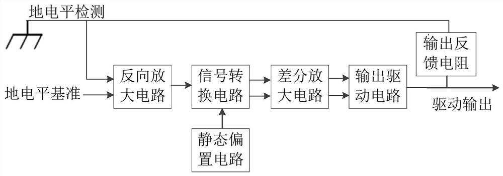
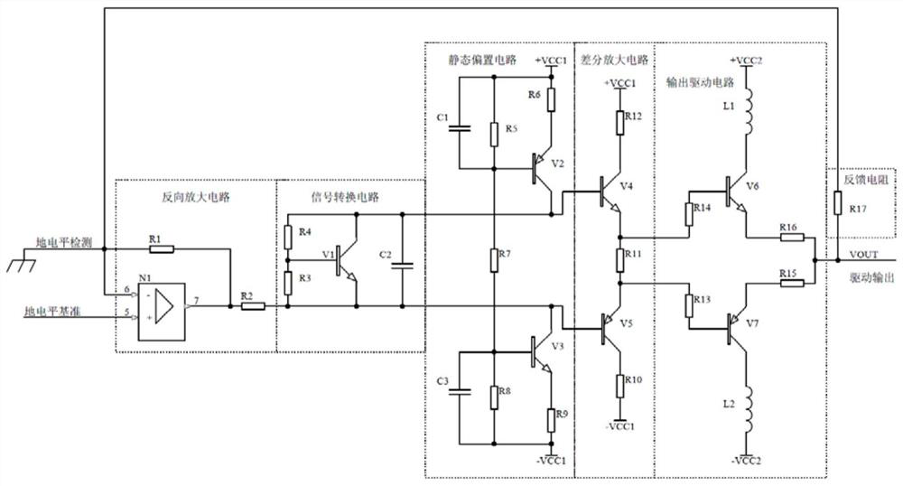
[0030] An active grounding circuit and method based on negative feedback loop control of the present invention is specifically a design and method of an active grounding circuit using negative feedback control technology. The circuit can quickly adjust the level fluctuation of the grounding system, and even when the level fluctuation of the grounding system is very weak, the negative feedback loop control circuit can also stably and reliably suppress the fluctuation. Compared with the traditional grounding circuit, this circuit has incomparable superiority, which improves the stability and reliability of the grounding circuit, especially the ability to suppress and adjust weak ground level fluctuations has a breakthrough, which effectively improves the testing equipment. ground level stability.

[0031] Such as figure 1 As shown, the active gr...


PUM


Abstract

The invention discloses an active grounding circuit and method based on negative feedback loop control, and belongs to the field of semiconductor testing and power supplies. The active grounding circuit comprises a reverse amplification circuit, a signal conversion circuit, a differential amplification circuit, an output driving circuit, a static bias circuit and an output feedback resistor, wherein the static working points of the signal conversion circuit and the differential amplification circuit are adjusted through the static bias circuit, after the difference value of a detected ground level signal and a ground level reference signal is reversely amplified through the reverse amplification circuit, a single end is converted into a differential signal through the signal conversion circuit, the differential signal is further amplified by the differential amplification circuit and then is output to the output driving circuit, the output driving circuit converts the differential signal into a single-ended signal again, and then the signal is used for controlling the fluctuation of the ground level so as to ensure that the ground level is stably set to be 0V. According to the invention, a negative feedback loop control technology is adopted, so that the received level can be quickly and accurately adjusted to 0 V through reverse amplification regardless of the rising or falling of the grounding level.

Description

technical field [0001] The invention belongs to the field of semiconductor testing and power supply, and in particular relates to an active grounding circuit and method based on negative feedback loop control. Background technique [0002] With the rapid development of semiconductor testing technology, the development trend of semiconductor testing instruments and systems must be towards higher precision. The weak voltage fluctuation of the ground circuit of the power supply of the existing semiconductor testing instruments and testing systems will become a factor that affects the testing accuracy. Key factor. The grounding system of traditional test instruments is to connect the ground plane to a fixed level. Due to the resistance of the power supply output line, as the output current changes, the voltage on the line will change, and the level of the grounding system will also change. It will change accordingly, which will seriously affect the test accuracy and restrict th...

Claims


Application Information

Patent Timeline
Patent Type & Authority Applications(China)
IPC IPC(8): G05F1/56
CPCG05F1/561
Inventor 李雷张永坡王文廷李斌汪成龙颜魏伟戚瑞民王俊张奕杨小光
Owner THE 41ST INST OF CHINA ELECTRONICS TECH GRP
Why Eureka
Try Eureka