TSV multi-stress reliability test chip structure and device based on lead bonding

A chip structure and wire bonding technology, applied in the semiconductor field, can solve the problems of lack of experimental research, inability to realize multi-stress loading, etc., and achieve the effects of convenient use, scientific comprehensiveness, accuracy and reliability, and low cost.

Active Publication Date: 2021-10-01
NAT UNIV OF DEFENSE TECH
View PDF6 Cites 0 Cited by
  • Summary
  • Abstract
  • Description
  • Claims
  • Application Information

AI Technical Summary

Problems solved by technology

However, the current research on the reliability of TSV structures is basically based on finite element thermal simulation, and there is a lack of experimental research.
The few experimental studies have designed dedicated TSV test chips, and carried out thermal cycle and electrical bias tests on them, but these chips and test circuits cannot achieve multi-stress loading

Method used


Image

  • TSV multi-stress reliability test chip structure and device based on lead bonding
  • TSV multi-stress reliability test chip structure and device based on lead bonding
  • TSV multi-stress reliability test chip structure and device based on lead bonding

Examples


Embodiment approach

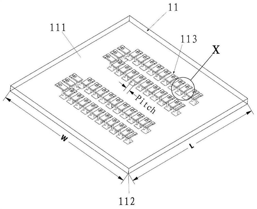
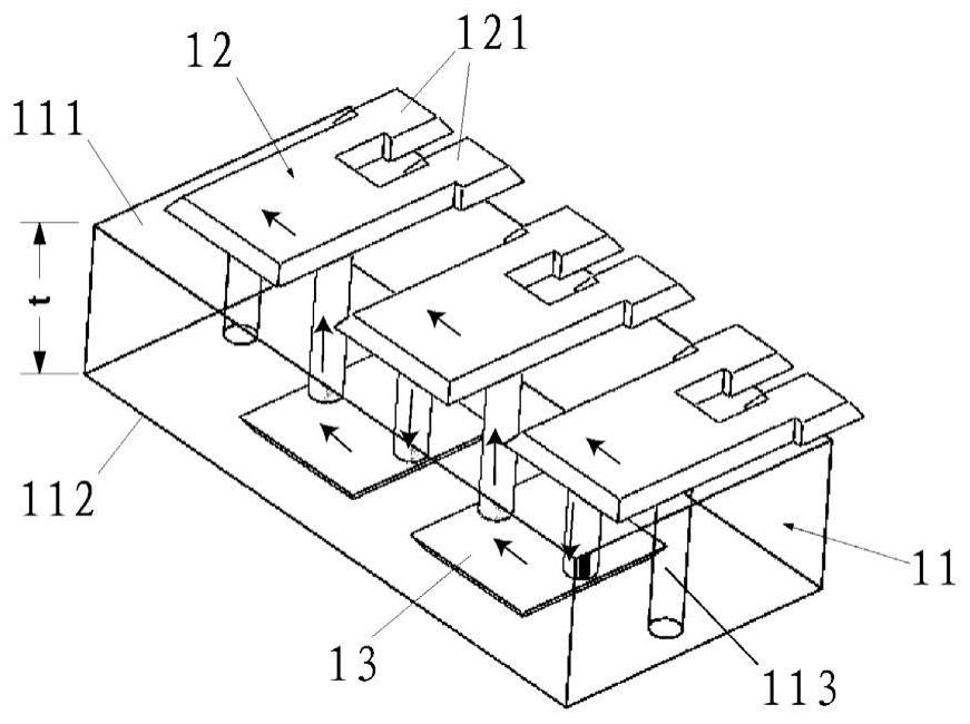
[0086] According to one embodiment of the present invention, both the chip structure with the daisy chain interconnection structure and the chip structure with the Kelvin chain interconnection structure in the present invention are taped out by designing a mask and adopting a mature process. Chips are taped out on the same wafer, and the corresponding chip die can be obtained after dicing. The outer size of the die is: L (length) × W (width) × t (thickness). In order to be able to directly load temperature and humidity to the TSV structure 113, the die is not packaged anymore. The chips are then tested and bad dies are eliminated.

[0087] The structure of the TSV multi-stress reliability test chip of the present invention can be connected to a digital acquisition system for testing after the electrodes are led out through the above-mentioned structure. Moreover, this solution realizes the reliability test in a multi-stress environment based on the above-mentioned structure. ...


PUM


Abstract

The invention relates to a TSV multi-stress reliability test chip structure and device based on lead bonding. The chip structure comprises a silicon substrate, a top electrode, and abottom electrode, wherein a plurality of TSV structures penetrating through the upper surface and the lower surface of the silicon substrate are arranged on the silicon substrate in an array manner; the top electrode is located on the upper surface of the silicon substrate and used for being connected with the top of the TSV structure; the bottom electrode is located on the lower surface of the silicon substrate and used for being connected with the bottom of the TSV structure; and the top electrode and the bottom electrode on the silicon substrate are selectively connected with the end parts of the TSV structures respectively to form a daisy chain interconnection structure or a Kelvin chain interconnection structure. The test device comprises a fixed supporting plate, a test circuit board, a multi-stress loading device, a signal acquisition device and the like. According to the scheme, multi-stress loading can be conveniently and comprehensively carried out on an actual single TSV or multiple TSV link structures, and the reliability of the TSV structure can be scientifically, comprehensively and accurately evaluated through a test means.

Description

technical field [0001] The invention relates to the field of semiconductors, in particular to a TSV multi-stress reliability test chip structure and device based on wire bonding. Background technique [0002] As the advanced chip manufacturing process moves towards 3nm, the density of transistors on the two-dimensional plane of the wafer is gradually approaching the physical limit, accompanied by a substantial increase in chip development costs and an extension of the development cycle. Thus, "Moore's Law" has failed. Therefore, a three-dimensional integrated package based on a through silicon via (Through silicon vias, TSV) structure emerges as the times require. Three-dimensional integrated packaging integrates wafers in the vertical direction through TSV and stacking, so as to obtain packaged chips with smaller size, higher bandwidth, lower latency, and higher performance, and can also be integrated with microelectromechanical systems (MEMS) Realize heterogeneous integr...

Claims


Application Information

Patent Timeline
Patent Type & Authority Applications(China)
IPC IPC(8): H01L23/522G01R31/28H01L21/66
CPCH01L23/5226H01L22/30G01R31/2862G01R31/2874G01R31/2881
Inventor 范政伟陈循刘泰成蒋瑜张书锋汪亚顺
Owner NAT UNIV OF DEFENSE TECH
Why Eureka
Try Eureka