Composite samples and methods for their preparation

A sample and substrate technology, applied in the field of combined samples and its preparation, can solve problems such as misoperation and time-consuming

Active Publication Date: 2022-06-07
YANGTZE MEMORY TECH CO LTD
View PDF7 Cites 0 Cited by
  • Summary
  • Abstract
  • Description
  • Claims
  • Application Information

AI Technical Summary

Problems solved by technology

[0004] However, in the related art, there are many and complicated steps for preparing thinned samples, which is easy to cause misoperation and takes a long time.

Method used


Image

  • Composite samples and methods for their preparation
  • Composite samples and methods for their preparation
  • Composite samples and methods for their preparation

Examples


preparation example Construction

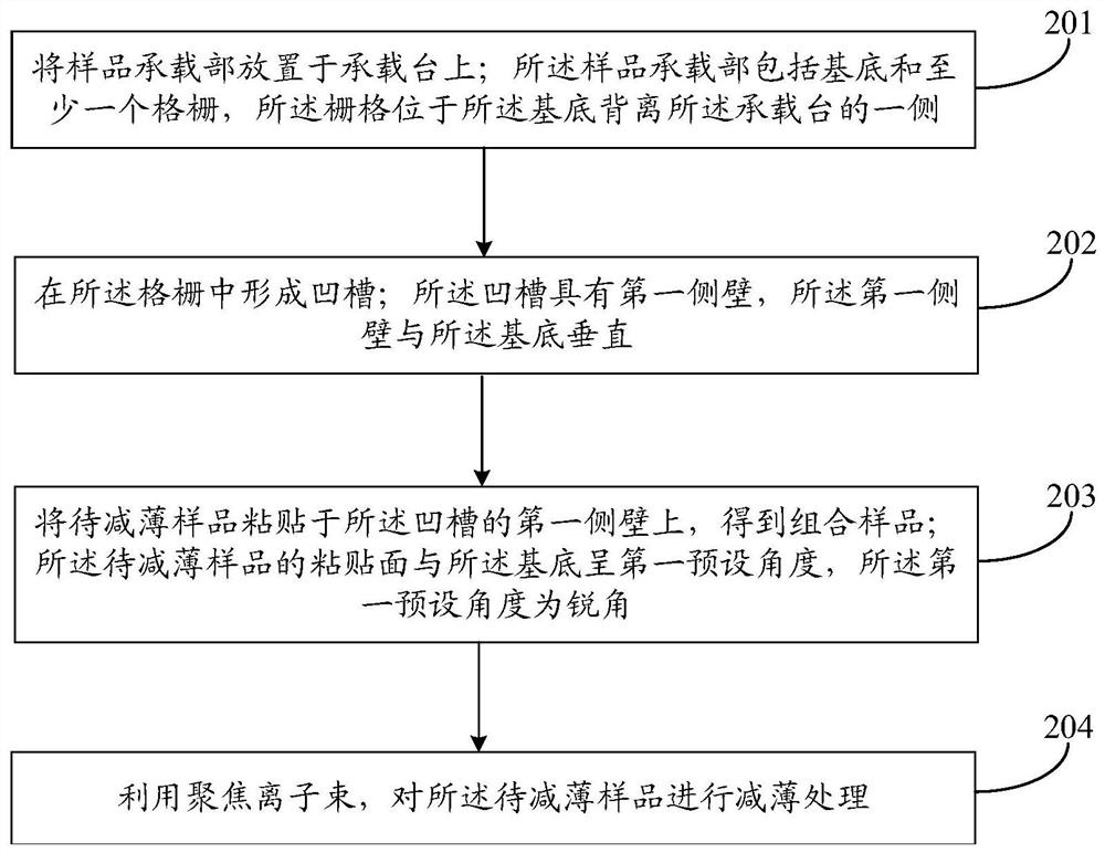
[0060] The embodiments of the present application provide a method for preparing a combined sample, figure 2 This is a schematic diagram of the realization flow of a method for preparing a combined sample provided in the embodiment of the present application. like figure 2 As shown, the method includes the following steps:

[0061] Step 201 : placing the sample carrying part on the carrying table; the sample carrying part includes a vertical base and at least one grid, and the grid is located on the side of the base away from the carrying table;

[0062] Step 202: forming a groove in the grid; the groove has a first side wall, and the first side wall is perpendicular to the base;

[0063] Step 203: Paste the sample to be thinned on the first side wall of the groove to obtain a combined sample; the adhesive surface of the sample to be thinned and the substrate are at a first preset angle, and the first preset angle is Let the angle be an acute angle;

[0064] Step 204 : u...


PUM

PropertyMeasurementUnit
thicknessaaaaaaaaaa

Abstract

The embodiment of the present application discloses a combined sample and a preparation method thereof, wherein the preparation method includes: placing the sample carrying part on a carrying platform; the sample carrying part includes a base and at least one grid, and the grid is located on the The base is away from the side of the carrying platform; a groove is formed in the grid; the groove has a first side wall, and the first side wall is perpendicular to the base; the sample to be thinned is pasted on On the first side wall of the groove, a combined sample is obtained; the sticking surface of the sample to be thinned and the substrate form a first preset angle, and the first preset angle is an acute angle; using a focused ion beam, Thinning treatment is performed on the sample to be thinned.

Description

technical field [0001] The present application relates to the field of semiconductor technology, and in particular, to a composite sample and a preparation method thereof. Background technique [0002] Today, with the continuous development of semiconductor technology, due to the continuous reduction of the size of semiconductor devices, the difficulty of analyzing the causes of their failures has also become more and more difficult. , can observe the internal structure and crystal defects of semiconductor devices, and can conduct contrast imaging and electron diffraction research on the same area, and connect the topographic information with the structural information, so it has become an indispensable part of the failure analysis of semiconductor devices. important means. [0003] Since the TEM uses the electron beam that penetrates the sample to image, and the electron itself has a very weak penetrating ability, the TEM sample, especially the part that needs to be observ...

Claims


Application Information

Patent Timeline
Patent Type & Authority Patents(China)
IPC IPC(8): G01N23/20008G01N23/04G01N23/20025G01N23/20058G01N1/28
CPCG01N23/20008G01N23/04G01N23/20025G01N23/20058G01N1/28G01N2223/03G01N2223/0565G01N2223/102
Inventor 董旭林郭伟
Owner YANGTZE MEMORY TECH CO LTD
Why Eureka
Try Eureka