
Piezoelectric wafer active sensor packaging structure

A piezoelectric chip and packaging structure technology, applied in the manufacture/assembly of piezoelectric/electrostrictive devices, piezoelectric/electrostrictive/magnetostrictive devices, circuits, etc., can solve the problem of large environmental factors and waiting time Long, piezoelectric chip active sensor damage and other issues, to speed up installation efficiency and improve durability

Pending Publication Date: 2021-09-28
DALIAN UNIV OF TECH
View PDF0 Cites 0 Cited by
  • Summary
  • Abstract
  • Description
  • Claims
  • Application Information

AI Technical Summary

Problems solved by technology

[0003] 1) Due to improper operation during the installation process, the piezoelectric chip active sensor may be damaged, resulting in performance defects;
[0004] 2) The pasting operation requires experienced operators to carry out on-site, and the pressure needs to be maintained for a long time to ensure the conductivity, and the waiting time is long;
[0006] 4) The performance of the adhesive layer is greatly affected by environmental factors (temperature, humidity), and it is difficult to ensure the quality of the paste;
[0007] 5) The quality of solder joints is difficult to ensure consistency, and it is difficult to ensure the quality of welding;
[0008] 6) The piezoelectric chip active sensor is exposed to harsh environments during use, which can easily cause damage to the piezoelectric chip active sensor;

Method used


Image

  • Piezoelectric wafer active sensor packaging structure
  • Piezoelectric wafer active sensor packaging structure
  • Piezoelectric wafer active sensor packaging structure

Examples


Embodiment Construction

[0025] The specific implementation manners of the present invention will be further described below in conjunction with the accompanying drawings and technical solutions.

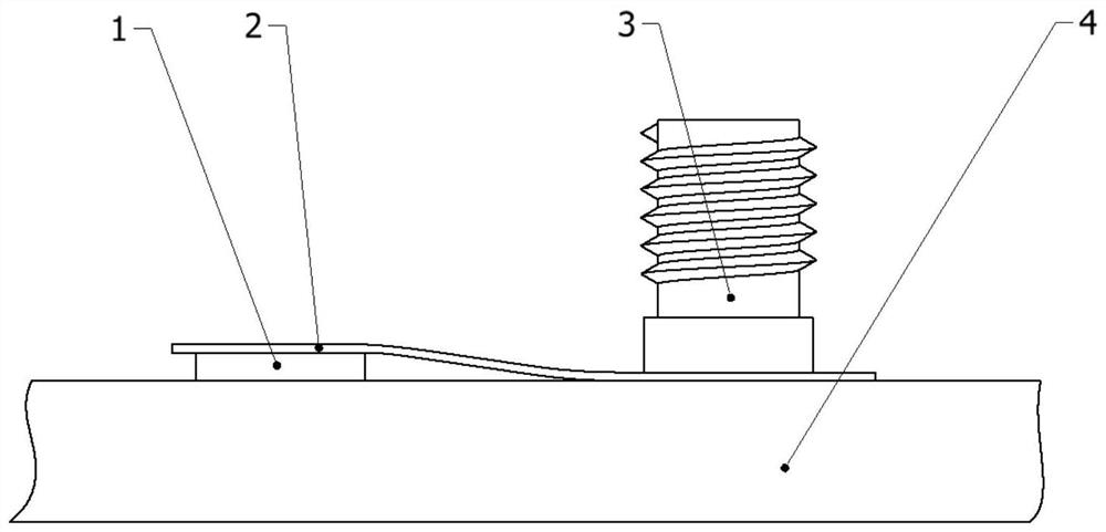
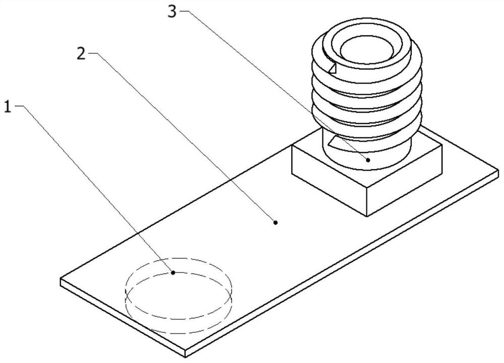
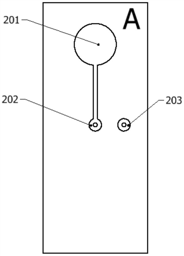
[0026] The present invention utilizes a flexible printed circuit (Flexible Printed Circuit, FPC), which uses an insulating flexible film 208 as a base material, forms a metal layer on both surfaces of the flexible film by electroplating or deposition, and makes printed circuits A210 and A210 respectively. Printed Circuits B211. The thickness of the flexible circuit board 2 is less than 0.15mm. The invention includes a flexible circuit board 2 with a printed circuit, a piezoelectric chip active sensor 1 and a radio frequency coaxial adapter 3 .

[0027] A packaging method and packaging structure of a piezoelectric wafer active sensor of the present invention will be further described in detail below in conjunction with the accompanying drawings.

[0028] refer to image 3 , Figure 4 Different printed ci...


PUM

PropertyMeasurementUnit
thicknessaaaaaaaaaa

Abstract

The invention provides a piezoelectric wafer active sensor packaging structure, and belongs to the technical field of electromechanical impedance. The piezoelectric wafer active sensor packaging structure comprises a flexible circuit board, a piezoelectric wafer active sensor and a radio frequency coaxial adapter; an insulated flexible film is used as a base material, metal layers are formed on the two surfaces of the flexible film in an electroplating or deposition mode, and a printed circuit is manufactured; the piezoelectric wafer active sensor and the radio frequency coaxial adapter are installed on the flexible circuit board, and the three are electrically connected; and the piezoelectric wafer active sensor is packaged, so that the test can be completed without adhering or welding a test signal line on the surface of the piezoelectric wafer active sensor, the direct interconnection of the piezoelectric wafer active sensor and a test instrument is realized, the installation efficiency of the piezoelectric wafer active sensor is accelerated, and due to protection of the flexible film, the durability of the piezoelectric wafer active sensor is improved.

Description

technical field [0001] The invention belongs to the technical field of electromechanical impedance, and relates to a piezoelectric chip active sensor packaging structure. Background technique [0002] At present, electromechanical impedance technology is a relatively good detection method that has high measurement accuracy, does not destroy the integrity of the monitored structure, and does not damage or affect the future performance or use of the monitored structure. The electromechanical impedance technology is a technology that uses the piezoelectric chip active sensor to be glued to the surface of the measured structure with epoxy resin to detect or monitor the measured structure, that is, to use the positive and negative piezoelectric effect and electromechanical coupling characteristics of the piezoelectric chip Obtain mechanical impedance information of the structure under test. During the electromechanical impedance test, the test signal line is drawn out from the e...

Claims


Application Information

Patent Timeline
Patent Type & Authority Applications(China)
IPC IPC(8): H01L41/053H01L41/23H10N30/88H10N30/02
CPCH10N30/88H10N30/02
Inventor 孙清超袁志伟王瑞强姜海涛付雨露
Owner DALIAN UNIV OF TECH
Learn More