Printed circuit board, finished circuit board and welding method

A technology of printed circuit boards and circuit boards, applied in the direction of printed circuits, printed circuit manufacturing, printed circuit components, etc., can solve problems such as poor welding, and achieve the effect of solving poor welding

Active Publication Date: 2021-09-17
SHENZHEN RUIKE HUILIAN TECH
View PDF11 Cites 0 Cited by
  • Summary
  • Abstract
  • Description
  • Claims
  • Application Information

AI Technical Summary

Problems solved by technology

[0006] The invention provides a printed circuit board, a finished circuit board and a welding method to solve the problem of soldering caused by drift or tin-climbing effect in the prior art when soldering small-sized electronic devices on overlapping pads of compatible design printed circuit boards. bad question

Method used


Image

  • Printed circuit board, finished circuit board and welding method
  • Printed circuit board, finished circuit board and welding method
  • Printed circuit board, finished circuit board and welding method

Examples


Embodiment

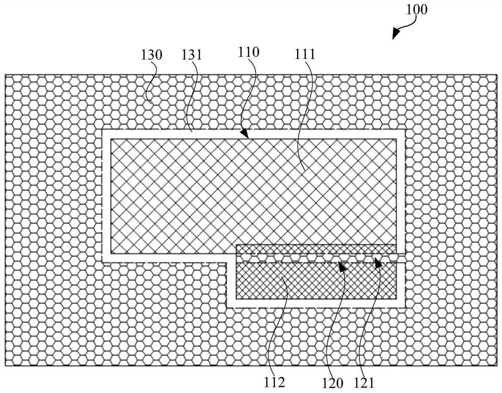
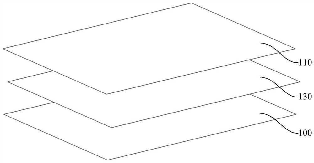
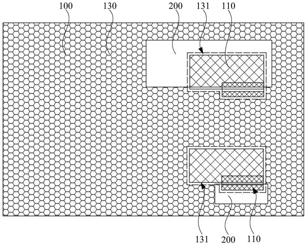
[0040] figure 1 The structural representation of the printed circuit board provided by the present invention, figure 2 A schematic diagram of the composition and structure of the printed circuit board provided by the present invention, image 3 The structural representation of the finished circuit board provided by the present invention, Figure 4 It is a schematic diagram of the soldering positions of two electronic devices on the finished circuit board provided by the present invention.

[0041] Such as Figure 1-4 As shown, a printed circuit board provided by the present invention includes a circuit board body 100 and at least one composite pad 110 located on the circuit board body 100. The composite pad 110 has a slit 120 to divide the composite pad 110 into The first soldering portion 111 and the second soldering portion 112 are connected to each other; the gap 120 is covered with a soldering resist 121; The window 131 corresponding to the second welding portion 112 ...


PUM


Abstract

The invention provides a printed circuit board, a finished circuit board and a welding method, the printed circuit board comprises a circuit board body and a composite bonding pad located on the circuit board body, and the composite bonding pad is provided with a gap so as to divide the composite bonding pad into a first welding part and a second welding part which are connected with each other. The gap is covered with a solder resist part; the surface of the circuit board body is covered with a solder mask, and the solder mask is provided with a window to expose the first welding part and the second welding part; the first welding part is used for welding a pin of a first electronic device; the second welding part is used for welding a pin of a second electronic device. According to the printed circuit board provided by the invention, the problem of poor welding caused by a drifting or tin climbing effect when electronic devices with relatively small sizes are welded on overlapped bonding pads in the prior art is solved.

Description

technical field [0001] The invention relates to the technical field of circuit board production, in particular to a printed circuit board, a finished circuit board and a welding method. Background technique [0002] With the rapid development of electronic technology and the continuous improvement of manufacturing technology, the finished circuit board (PCBA) is also developing towards high density. It is bound to put forward higher requirements for the manufacturability of the product design, if there is an unreasonable design, it will definitely have a serious impact on the manufacturability of the product. [0003] In the process of designing a printed circuit board (PCB), it is usually necessary to realize different requirements on the same single board for compatible design. Due to the limitation of the printed circuit board space, in order to achieve high density of compatible electronic devices, the pads of the electronic devices are generally arranged to be stacked ...

Claims


Application Information

Patent Timeline
Patent Type & Authority Applications(China)
IPC IPC(8): H05K1/11H05K3/34
CPCH05K1/111H05K3/341
Inventor 王克伟
Owner SHENZHEN RUIKE HUILIAN TECH
Why Eureka
Try Eureka