Formation method of semiconductor structure and semiconductor structure

A semiconductor and stacked structure technology, which is applied in semiconductor devices, semiconductor/solid-state device manufacturing, transistors, etc., can solve the problems of poor lateral stability in the capacitor array area, and achieve the effects of improving electrical performance, increasing capacitance value, and improving stability

Inactive Publication Date: 2021-09-17
CHANGXIN MEMORY TECH INC
View PDF3 Cites 1 Cited by
  • Summary
  • Abstract
  • Description
  • Claims
  • Application Information

AI Technical Summary

Problems solved by technology

[0005] The invention provides a method for forming a semiconductor structure and a semiconductor structure, which are used to solve the problem of poor lateral stability of the capacitor array region in the existing semiconductor structure, so as to reduce the risk of collapse or overturning of the lower electrode and improve the performance of the semiconductor device stability

Method used


Image

  • Formation method of semiconductor structure and semiconductor structure
  • Formation method of semiconductor structure and semiconductor structure
  • Formation method of semiconductor structure and semiconductor structure

Examples


Embodiment Construction

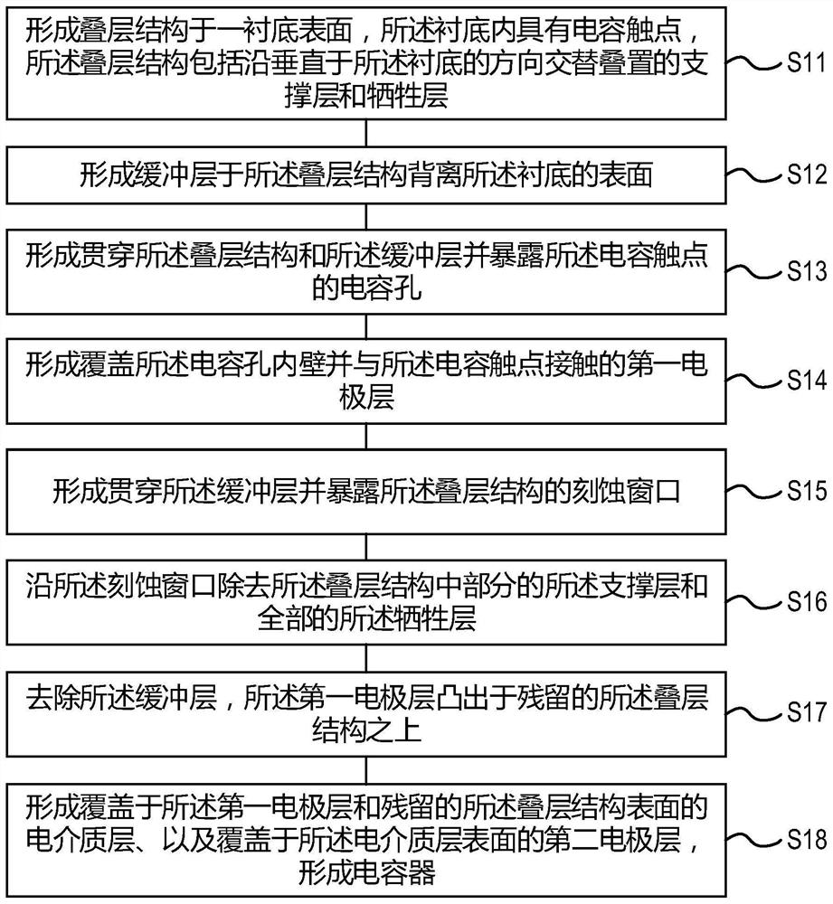
[0044] The method for forming the semiconductor structure provided by the present invention and the specific implementation of the semiconductor structure will be described in detail below in conjunction with the accompanying drawings.

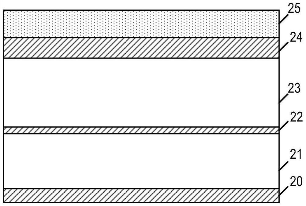
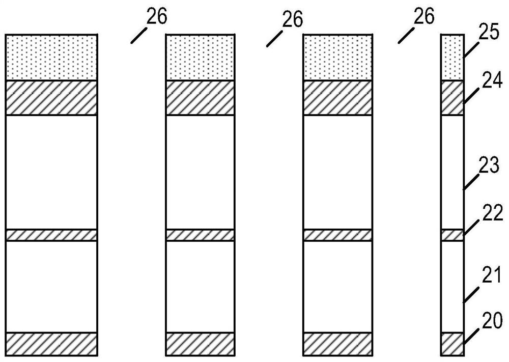
[0045] This specific embodiment provides a method for forming a semiconductor structure, with figure 1 It is a flowchart of a method for forming a semiconductor structure in a specific embodiment of the present invention, with Figures 2A-2P It is a schematic cross-sectional view of the main process in the process of forming the semiconductor structure according to the specific embodiment of the present invention. like figure 1 , Figure 2A-Figure 2P As shown, the method for forming a semiconductor structure provided in this specific embodiment includes the following steps:

[0046] Step S11, forming a stacked structure on the surface of a substrate, the substrate has capacitive contacts, and the stacked structure includes alternately stack...


PUM


Abstract

The invention provides a semiconductor structure forming method and a semiconductor structure. The forming method of the semiconductor structure comprises the following steps: forming a laminated structure on the surface of a substrate, wherein the laminated structure comprises supporting layers and sacrificial layers which are alternately laminated; forming a buffer layer on the surface, deviating from the substrate, of the laminated structure; forming a capacitor hole which penetrates through the laminated structure and the buffer layer and exposes the capacitor contact; forming a first electrode layer covering the inner wall of the capacitor hole; forming an etching window penetrating through the buffer layer; removing a part of the supporting layer and all the sacrificial layers in the laminated structure along the etching window; removing the buffer layer, wherein the first electrode layer protrudes out of the residual laminated structure; and forming a dielectric layer and a second electrode layer to form a capacitor. According to the invention, the transverse stability of the capacitor array area is improved, and the capacitance value of the capacitor can be effectively improved.

Description

technical field [0001] The invention relates to the technical field of semiconductor manufacturing, in particular to a method for forming a semiconductor structure and the semiconductor structure. Background technique [0002] A dynamic random access memory (Dynamic Random Access Memory, DRAM) is a semiconductor structure commonly used in electronic devices such as computers, and is composed of a plurality of storage units, and each storage unit usually includes a transistor and a capacitor. The gate of the transistor is electrically connected to the word line, the source is electrically connected to the bit line, and the drain is electrically connected to the capacitor. The word line voltage on the word line can control the opening and closing of the transistor, so that the stored data can be read through the bit line. Data information in the capacitor, or write data information into the capacitor. [0003] As semiconductor devices shrink in size, their lateral area on a s...

Claims


Application Information

Patent Timeline
Patent Type & Authority Applications(China)
IPC IPC(8): H01L21/8242H01L27/108
CPCH10B12/03H10B12/30H01L28/91H01L28/92H01L28/86H01L21/32139
Inventor 陆勇
Owner CHANGXIN MEMORY TECH INC
Why Eureka
Try Eureka