Light-emitting device

A technology for light-emitting devices and light-emitting elements, which is applied to electrical components, electric solid-state devices, circuits, etc., and can solve problems such as electrical anomalies, the inability to further increase the layout density of light-emitting transistors, and the difficulty of making light-emitting devices.

Pending Publication Date: 2021-09-14
陈冠宇 +2
View PDF8 Cites 2 Cited by
  • Summary
  • Abstract
  • Description
  • Claims
  • Application Information

AI Technical Summary

Problems solved by technology

Therefore, electrical abnormalities are likely to occur in the die-bonding process and the wire bonding process, thus increasing the difficulty of the manufacturing process of the light-emitting device and reducing the yield of the manufacturing process
In addition, the layout density of light-emitting transistors cannot be further improved because the wire bonding process requires additional wiring space for arranging electrodes.

Method used


Image

  • Light-emitting device
  • Light-emitting device
  • Light-emitting device

Examples


Embodiment Construction

[0017] Reference will now be made in detail to the exemplary embodiments of the present invention, examples of which are illustrated in the accompanying drawings. However, the present invention can also be embodied in various forms and should not be limited to the embodiments described herein. The thicknesses of layers and regions in the drawings may be exaggerated for clarity. Wherever possible, the same reference numbers are used in the drawings and descriptions to refer to the same or like parts.

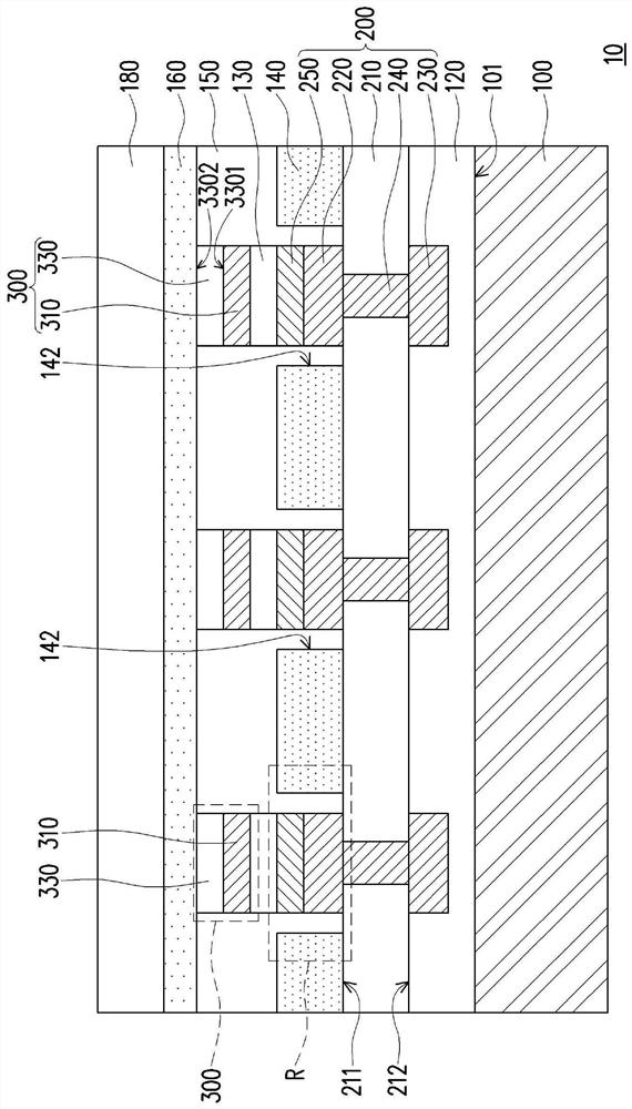
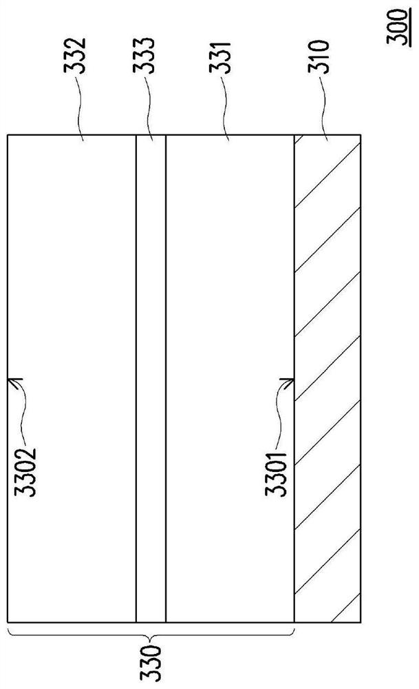
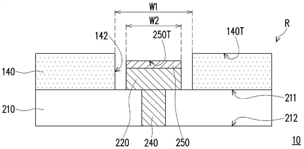
[0018] figure 1 is a schematic cross-sectional view of a light emitting device according to an embodiment of the present invention. figure 2 is a schematic cross-sectional view of a light-emitting element according to an embodiment of the present invention. Figure 3A yes figure 1 The partial cross-sectional enlarged schematic diagram of the region R of the light-emitting device. For the clarity of the diagram and the convenience of explanation, figure 1 , figure 2 and ...


PUM


Abstract

A light-emitting device including a substrate, an insulating layer, an inner circuit structure, a plurality of light-emitting elements, an insulating encapsulation layer, and a transparent conductive layer is provided. The insulating layer is disposed on the substrate. The inner circuit structure is disposed on the insulating layer. The light-emitting elements are correspondingly disposed on the inner circuit structure. The insulating encapsulation layer is disposed on the inner circuit structure. The insulating encapsulating layer covers a portion of the inner circuit structure and encapsulates the light-emitting elements. The transparent conductive layer is disposed on the insulating encapsulating layer. The transparent conductive layer electrically connects the light-emitting elements, and serially connects the light-emitting elements.

Description

technical field [0001] Embodiments of the present invention relate to a light emitting device. Background technique [0002] With the improvement of manufacturing technology, the light emitting transistor (Light Emitting Diode, LED) has gradually enhanced its luminous efficiency and brightness through continuous research and development, so as to expand and adapt to the needs of various products. However, under the pursuit of reducing the size of the light-emitting transistor and increasing the power and operating current, the light-emitting transistor will relatively generate more heat, which will affect its performance. [0003] In addition, such as submillimeter or micro light-emitting transistors (mini LED or micro LED) are very small in size. Therefore, electrical abnormalities are likely to occur in the die-bonding process and the wire bonding process, thereby increasing the difficulty of the manufacturing process of the light emitting device and reducing the yield of...

Claims


Application Information

Patent Timeline
Patent Type & Authority Applications(China)
IPC IPC(8): H01L33/48H01L33/52H01L33/64H01L27/15
CPCH01L33/48H01L33/52H01L33/641H01L33/647H01L27/156H01L25/167H01L25/0753H01L33/62H01L33/56H01L33/54
Inventor 陈冠宇林晓龙黄浩祥
Owner 陈冠宇
Why Eureka
Try Eureka