
Method for epitaxially growing InGaAs film on GaP/Si substrate and InGaAs film

An epitaxial growth and substrate technology, applied in the field of InGaAs thin films, can solve the problems of reducing the quality of thin film crystals, large residual stress, large lattice mismatch, etc., to solve the problem of lattice matching, high crystal quality, good stress relief. Effect

Pending Publication Date: 2021-08-27
SUZHOU INST OF NANO TECH & NANO BIONICS CHINESE ACEDEMY OF SCI
View PDF0 Cites 0 Cited by
  • Summary
  • Abstract
  • Description
  • Claims
  • Application Information

AI Technical Summary

Problems solved by technology

However, since Si and In x Ga 1-x There is a large lattice mismatch between As films. If In is grown directly on the Si substrate x Ga 1-x As thin film, then due to the lattice mismatch between the two will lead to large residual stress
On the one hand, large residual stress may make In x Ga 1-x As film grows with cracks or even cracks
On the other hand, a large residual stress will make In x Ga 1-x A large number of defects are generated in the As film, thereby reducing the crystal quality of the film and increasing the surface roughness of the film, which will eventually reduce the device life and deteriorate the device performance

Method used


Image

  • Method for epitaxially growing InGaAs film on GaP/Si substrate and InGaAs film
  • Method for epitaxially growing InGaAs film on GaP/Si substrate and InGaAs film
  • Method for epitaxially growing InGaAs film on GaP/Si substrate and InGaAs film

Examples


Embodiment Construction

[0022] Hereinafter, specific embodiments of the present invention will be described in detail with reference to the accompanying drawings. This invention may, however, be embodied in many different forms and should not be construed as limited to the specific embodiments set forth herein. Rather, the embodiments are provided to explain the principles of the invention and its practical application, thereby enabling others skilled in the art to understand the invention for various embodiments and with various modifications as are suited to particular intended uses.

[0023] As used herein, the term "comprising" and its variants represent open terms meaning "including but not limited to". The terms "based on", "based on", etc. mean "based at least in part on", "based on at least in part". The terms "one embodiment" and "an embodiment" mean "at least one embodiment." The term "another embodiment" means "at least one other embodiment." The terms "first", "second", etc. may refer ...


PUM

PropertyMeasurementUnit
surface roughnessaaaaaaaaaa

Abstract

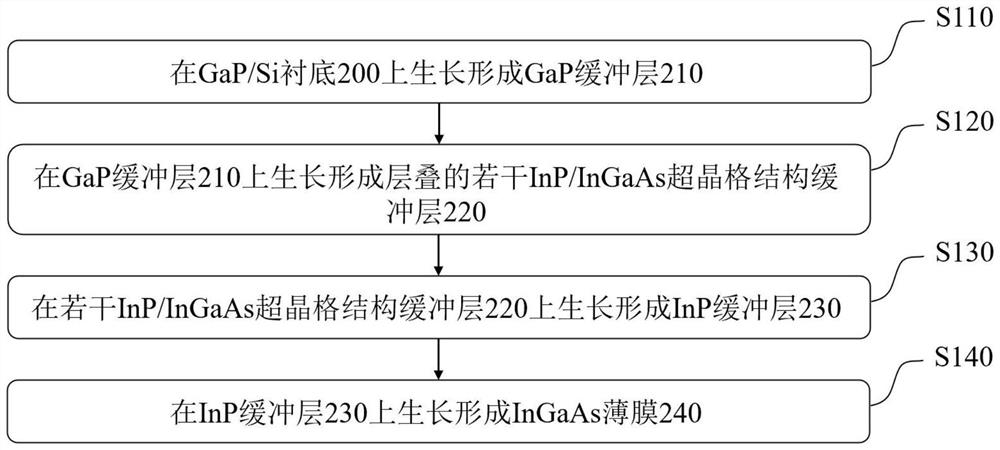
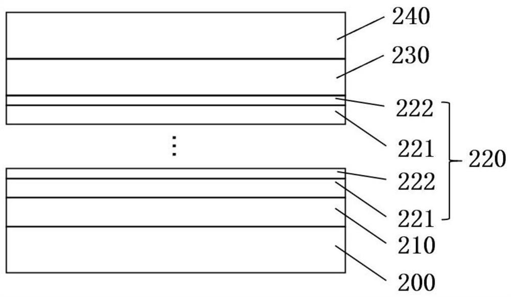
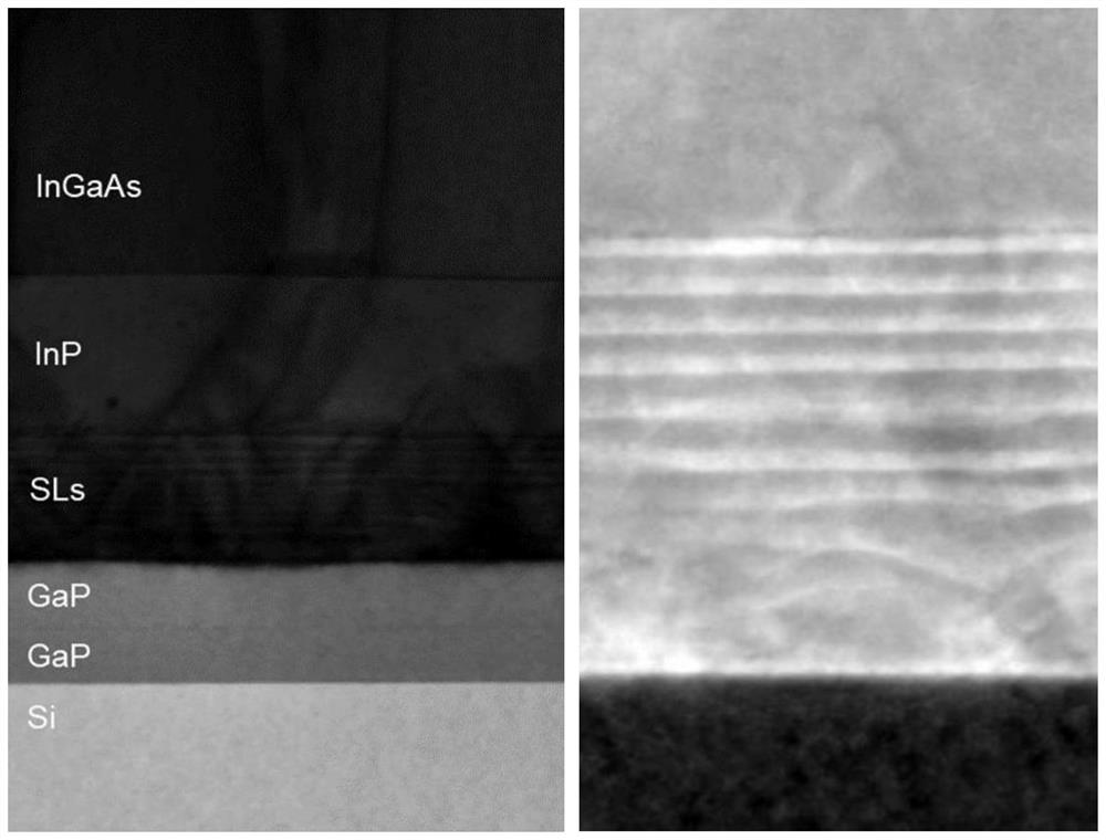
The invention provides a method for epitaxially growing an InGaAs thin film on a GaP / Si substrate. The method comprises the following steps of growing and forming a GaP buffer layer on the GaP / Si substrate; growing and forming a plurality of stacked InP / InGaAs superlattice structure buffer layers on the GaP buffer layer; growing and forming an InP buffer layer on the plurality of InP / InGaAs superlattice structure buffer layers; and growing and forming an InGaAs thin film on the InP buffer layer. In the invention, the GaP buffer layer, the InP / InGaAs superlattice structure buffer layer and the InP buffer layer are epitaxially grown on the GaP / Si substrate, so that the buffer layer with high crystal quality can be obtained, the lattice matching problem of the Si substrate and the InGaAs thin film is solved, dislocation caused by lattice mismatching between the substrate and the InGaAs thin film is effectively filtered, and the stress is better released.

Description

technical field [0001] The invention belongs to the technical field of semiconductor compound preparation, and in particular relates to a method for epitaxially growing an InGaAs thin film on a GaP / Si substrate and the InGaAs thin film epitaxially grown by the method. Background technique [0002] Group III-V compounds are widely used in optoelectronic devices due to their advantages of good stability, small effective mass, high electron mobility and peak velocity, and high light absorption coefficient. Among these III-V compounds, In x Ga 1-x The forbidden band width of As (0≤x≤1) compound can vary in the range of 0.35eV-1.43eV with the change of In composition. According to such characteristics, In x Ga 1-x As (0≤x≤1) compounds are widely used in optoelectronic semiconductor devices such as high electron mobility transistors, photodiodes, detectors, and solar cells. [0003] Epitaxial growth In x Ga 1-x As thin films often use InP and GaAs as substrates. However, I...

Claims


Application Information

Patent Timeline
Patent Type & Authority Applications(China)
IPC IPC(8): H01L21/02H01L29/201C30B25/18C30B29/40C30B29/44
CPCH01L21/02381H01L21/02461H01L21/02463H01L21/02507H01L21/02546H01L21/0262H01L29/201C30B25/183C30B29/40C30B29/44Y02P70/50
Inventor 魏铁石李雪飞陆书龙吴渊渊杨文献张雪孙强健邢志伟
Owner SUZHOU INST OF NANO TECH & NANO BIONICS CHINESE ACEDEMY OF SCI
Learn More