Blind buried hole circuit board laser target fool-proof design method
A technology of laser target and design method, which is applied in the directions of printed circuit, printed circuit manufacturing, and the formation of electrical connection of printed components, can solve the problems of increasing the difficulty factor, no fool-proof design, difficulty in positioning and grasping, and difficulty in manufacturing, etc. To achieve the effect of reducing the difficulty of grasping, reducing the difficulty of production, and facilitating the grasping and positioning operation
- Summary
- Abstract
- Description
- Claims
- Application Information
AI Technical Summary
Problems solved by technology
Method used
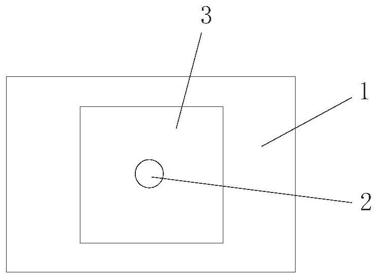
Image


Examples
Embodiment 1
[0037] The manufacturing method of a first-order blind buried circuit board shown in this embodiment includes the following processing steps in sequence:
[0038] (1) Cutting: Cut out the core board according to the panel size 520mm×620mm, the thickness of the core board is 0.5mm (excluding the outer copper thickness), and the thickness of the outer copper surface of the core board is 0.5oz (1oz≈35μm) .
[0039] (2), inner layer circuit production (negative film process): transfer of inner layer graphics, use vertical coating machine to coat photosensitive film, the film thickness of photosensitive film is controlled to 8 μm, adopt automatic exposure machine, with 6-8 grid exposure ruler ( 21-grid exposure ruler) to complete the exposure of the inner layer circuit, and form the inner layer circuit pattern after development; inner layer etching, etch the exposed and developed core board to etch the inner layer circuit, the inner layer line width is measured as 3mil, and it is i...
Embodiment 2
[0055] A method for manufacturing a second-order blind-buried circuit board shown in this embodiment, on the basis of the method described in Embodiment 1, when making the circuit in step (6), the two surfaces of the first sub-board are combined Four laser targets that overlap with the first laser target and the second laser target are produced on the upper and lower sides, that is, a set of first laser targets and a set of second laser targets are produced, and two layers of the first laser target are overlapped up and down. The targets are arranged adjacently, and the upper and lower layers of the second laser target are arranged adjacently; and the following processing steps are also included between steps (6) and (7):
[0056] (61) Lamination: The browning speed is browned according to the thickness of the bottom copper copper, and the outer copper foil, prepreg, first sub-board, prepreg, and outer copper foil are laminated in sequence according to the requirements, and the...
PUM
 Abstract
Description
Claims
Application Information
 - R&D
- Intellectual Property
- Life Sciences
- Materials
- Tech Scout
- Unparalleled Data Quality
- Higher Quality Content
- 60% Fewer Hallucinations
Browse by: Latest US Patents, China's latest patents, Technical Efficacy Thesaurus, Application Domain, Technology Topic, Popular Technical Reports.
© 2025 PatSnap. All rights reserved.Legal|Privacy policy|Modern Slavery Act Transparency Statement|Sitemap|About US| Contact US: help@patsnap.com