
Patterned substrate for LED growth, epitaxial wafer and preparation method of patterned substrate

A technology of patterned substrate and patterned sapphire, applied in electrical components, circuits, semiconductor devices, etc., can solve the problems of reduced crystal quality, easy cracking, inconsistent grain orientation, etc.

Inactive Publication Date: 2021-08-13
广东中图半导体科技股份有限公司
View PDF7 Cites 2 Cited by
  • Summary
  • Abstract
  • Description
  • Claims
  • Application Information

AI Technical Summary

Problems solved by technology

[0005] (1) The GaN epitaxial layer is directly grown on the flat sapphire substrate. When the thickness exceeds the critical thickness, cracks are prone to occur; on the other hand, the larger c-plane region has a higher density of GaN island growth, a greater number of Grain-bonded boundaries eventually lead to higher dislocation density, reducing the internal quantum efficiency of the LED;
[0006] (2) GaN epitaxial layer is grown directly on the pyramidal convex patterned sapphire substrate (PSS), GaN will still grow on the sidewall of the pyramid of PSS, and the grain orientation of different sidewalls is inconsistent, which is different from the bottom c-plane The merger of the grown GaN leads to the generation of dislocations and reduces the quality of the crystal;
The lateral growth of the epitaxial layers merges with each other and covers the pit area of ​​NPSS, but obvious air cavities and new dislocations will be formed under the merged area, and the air cavities are not conducive to the light extraction of flip-chip LEDs

Method used


Image

  • Patterned substrate for LED growth, epitaxial wafer and preparation method of patterned substrate
  • Patterned substrate for LED growth, epitaxial wafer and preparation method of patterned substrate
  • Patterned substrate for LED growth, epitaxial wafer and preparation method of patterned substrate

Examples


Embodiment Construction

[0032] In order to make the object, technical solution and advantages of the present invention clearer, specific embodiments of the present invention will be further described in detail below in conjunction with the accompanying drawings. It should be understood that the specific embodiments described here are only used to explain the present invention, but not to limit the present invention.

[0033] In addition, it should be noted that, for the convenience of description, only parts related to the present invention are shown in the drawings but not all content.

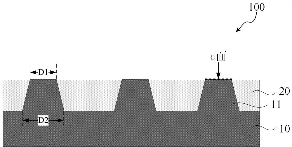
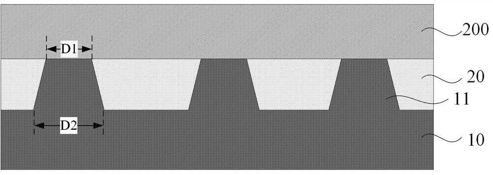
[0034] figure 1 A schematic structural diagram of a patterned substrate for LED growth provided by an embodiment of the present invention. Such as figure 1 As shown, the substrate 100 includes: a patterned sapphire substrate 10, a plurality of sapphire patterns 11 are formed on one side surface of the patterned sapphire substrate 10, the sapphire patterns 11 have a flat upper surface, and a heterogeneous layer 20 ...


PUM

PropertyMeasurementUnit
particle diameteraaaaaaaaaa
diameteraaaaaaaaaa
heightaaaaaaaaaa

Abstract

The embodiment of the invention discloses a patterned substrate for LED growth, an epitaxial wafer and a preparation method of the patterned substrate. The substrate comprises: a patterned sapphire substrate body, wherein a plurality of sapphire patterns are formed on the surface of one side of the patterned sapphire substrate body; and a heterogeneous layer located on the surface of the side, where the sapphire patterns are formed, of the patterned sapphire substrate body, wherein the sapphire patterns are wrapped in the heterogeneous layer, and the upper surfaces of the sapphire patterns are flush with the upper surface of the heterogeneous layer. The c surface of the sapphire is ground and polished, so that the material of the epitaxial layer only grows on the c surface of the sapphire in a nucleation manner, good flatness and controllable surface roughness are achieved, the epitaxial layer with low defects can be obtained, the dislocation density of the epitaxial layer is further reduced, and the epitaxial quality is guaranteed; and total reflection is reduced through gradient refractive index differences of the epitaxial layer, the sapphire substrate, the heterogeneous layer and air and a convex structure formed in the sapphire substrate, and the light extraction rate is increased, so that the external quantum efficiency is improved.

Description

technical field [0001] The embodiments of the present invention relate to the technical field of semiconductors, and in particular to a patterned substrate, an epitaxial wafer and a preparation method for LED growth. Background technique [0002] Light Emitting Diode (LED, Light Emitting Diode) has developed rapidly in recent years. LED has the advantages of small size, high efficiency, long life, environmental protection and energy saving. For example, under the condition of emitting the same luminous flux, the power consumption of LED is about 1 / 10 of that of incandescent lamp. Therefore, LED is known as a technology that "illuminates the future of mankind". With the breakthrough in the application of the third-generation semiconductor material gallium nitride (GaN), red light, blue light, white light, green light, and ultraviolet light-emitting diodes have come out one after another, and LEDs have gradually entered people's daily lives. At present, LED has been widely ...

Claims


Application Information

Patent Timeline
Patent Type & Authority Applications(China)
IPC IPC(8): H01L33/22H01L33/44H01L33/10H01L33/00
CPCH01L33/0066H01L33/10H01L33/22H01L33/44H01L2933/0008H01L2933/0025
Inventor 张剑桥谢鹏程米波肖桂明张小琼陆前军
Owner 广东中图半导体科技股份有限公司
Learn More