
RT detector suitable for epitaxial material and application thereof

A technology of epitaxial materials and detectors, which is applied in the direction of instruments, measuring devices, scientific instruments, etc., can solve the problems that the reflected signal exceeds the receiving range of the detector, the reflected signal exceeds the receiving range, and affects the accuracy, so as to realize the composition of the epitaxial layer and uniform growth control, avoid reflection signal out of control, and precisely control the effect of growth temperature

Inactive Publication Date: 2021-08-13
ZHONGSHAN DEHUA CHIP TECH CO LTD
View PDF7 Cites 0 Cited by
  • Summary
  • Abstract
  • Description
  • Claims
  • Application Information

AI Technical Summary

Problems solved by technology

[0003] Lattice-matched growth is a two-dimensional system produced by using heterostructures. It is mainly based on the fact that the atomic size of two different semiconductor materials is similar, so that semiconductor junctions close to perfect lattice matching can be produced, and the costs are not equal to each other. The meter energy levels will be aligned with each other when the junction is balanced, and cause discontinuity in the energy band, resulting in triangular potential energy at the junction; during the growth process, the thermal expansion coefficients of the epitaxial layer material and the substrate are different under high temperature conditions. The lower epitaxial wafer is warped, causing the reflected signal to exceed the receiving range of the detector, and the RT curve drops to zero, causing the temperature to run out of control
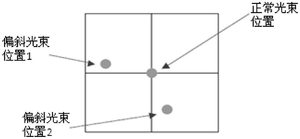
The schematic diagram of the cross-section of the position change of reflected light on different surfaces of the epitaxial wafer is shown in figure 1 ,like figure 1 As shown, the reflected beam on the flat surface ((A) or (D)) can be well received by the detector, but on the negatively inclined surface (B) and positively inclined surface (C), the reflected signal exceeds the acceptance range, In order to monitor the failure, the schematic diagram of the position of the reflected beam of the epitaxial wafer during the production process (top view) is shown in figure 2 ,like figure 2 As shown, when the surface of the epitaxial wafer is warped, part of the beam will deviate from the set position, thereby affecting the accuracy

Method used


Image

  • RT detector suitable for epitaxial material and application thereof
  • RT detector suitable for epitaxial material and application thereof
  • RT detector suitable for epitaxial material and application thereof

Examples


Embodiment 2

[0046] Embodiment 2 of the present invention is: a method for using an RT detector suitable for epitaxial materials, the method comprising the following steps:

[0047] placing the epitaxial wafer in the epitaxial wafer carrier, and controlling the motion state of the epitaxial wafer to be consistent with the carrier;

[0048] Adjust the monitoring mode in the RT detector according to the growth state of the epitaxial wafer to observe the growth process of the epitaxial wafer; wherein, the adjustment of the monitoring mode is to calculate the warping degree and Deformation feature, through the stepping motor to adjust the light direction of the eye-shaped light source.

Embodiment 3

[0049] Embodiment three of the present invention is: a method for using an RT detector suitable for epitaxial materials, the method comprising the following steps:

[0050] placing the epitaxial wafer in the epitaxial wafer carrier, and controlling the motion state of the epitaxial wafer to be consistent with the carrier;

[0051]Adjust the monitoring mode in the RT detector according to the growth state of the epitaxial wafer to observe the growth process of the epitaxial wafer; wherein, the adjustment of the monitoring mode is to calculate the degree of warpage and the intensity of the light received by the receiver. Deformation characteristics, change the position of light output by rotation, and record the direction of light output in polar coordinates.

[0052] The method for calculating the degree of warpage of the epitaxial wafers in Examples 2 and 3 of the present invention is as follows:

[0053] The position of the reflected light spot detected by the receiver is in...


PUM

PropertyMeasurementUnit
wavelengthaaaaaaaaaa

Abstract

The invention discloses an RT detector suitable for an epitaxial material and an application thereof. The RT detector comprises a light source and a receiver. The light source is in one-to-one correspondence with the receiver; the light source is used for emitting incident light, and the incident light is transmitted to the surface of an external epitaxial wafer to form an optical signal; the light source is in one-to-one correspondence with the external epitaxial wafer; the wavelength of the incident light is continuously adjustable; the shape of the light source is designed to be eyeball-shaped; the light source is connected with the power device through a transmission shaft; and a sub-receiver is used for receiving the optical signals formed by the corresponding epitaxial wafer and performing photoelectric conversion on the received optical signals to obtain electric signals. The detector can monitor the temperature of a slightly warped surface and accurately monitor the growth temperature in the production process of a lattice-matched epitaxial wafer.

Description

technical field [0001] The invention relates to the field of semiconductor material growth and preparation, in particular to an RT detector suitable for epitaxial materials and its application. Background technique [0002] The growth and preparation of epitaxial materials by MOCVD requires precise monitoring of the growth temperature. There are two commonly used monitoring methods, namely (RT) and (TC). Among them, RT is the temperature of the wafer surface, which is realized by monitoring the reflectance curve, and TC is the temperature of the graphite disk, which is detected by a thermocouple. [0003] Lattice-matched growth is a two-dimensional system produced by using heterostructures. It is mainly based on the fact that the atomic size of two different semiconductor materials is similar, so that semiconductor junctions close to perfect lattice matching can be produced, and the costs are not equal to each other. The meter energy levels will be aligned with each other ...

Claims


Application Information

Patent Timeline
Patent Type & Authority Applications(China)
IPC IPC(8): G01K11/125H01L31/12
CPCG01K11/125H01L31/125
Inventor 刘雪珍张小宾高熙隆黄珊珊杨文奕
Owner ZHONGSHAN DEHUA CHIP TECH CO LTD
Learn More