
A high-power silicon carbide diode and its manufacturing method

A technology of silicon carbide diodes and manufacturing methods, applied in the field of diodes, can solve the problems of unfavorable circuit board applications with multiple electronic components, easy winding of two gold wires, and large occupied area, so as to omit the welding process of gold wires and improve processing The effect of efficiency and simple structure

Active Publication Date: 2022-06-21
东莞市佳骏电子科技有限公司
View PDF5 Cites 0 Cited by
  • Summary
  • Abstract
  • Description
  • Claims
  • Application Information

AI Technical Summary

Problems solved by technology

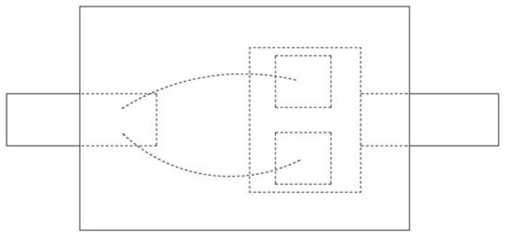
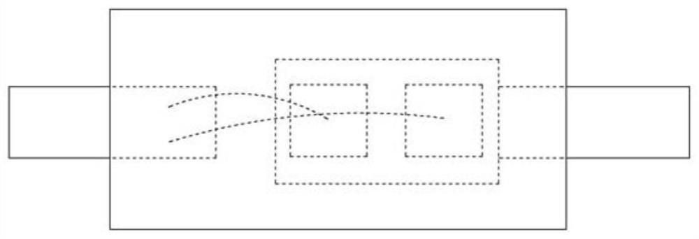
For this high-power silicon carbide diode, two silicon carbide chips are usually welded together on the same conductive plate, such as figure 2 The structure of the first conventional silicon carbide diode is shown. Two silicon carbide chips are arranged in the vertical direction of the figure, and then connected by two gold wires. The high-power silicon carbide diode made by this structure has a large vertical size. The area occupied by the application on the circuit board is large, which is not conducive to the application of circuit boards with multiple electronic components, such as image 3 The second conventional silicon carbide diode structure shown is to arrange two silicon carbide chips along the horizontal direction of the figure. Although the problem of large size can be solved, due to the intersection of the two gold wires, the two gold wires are easy to be wound during the plastic packaging process. , it is easy to cause defective products, and there are large defects

Method used


Image

  • A high-power silicon carbide diode and its manufacturing method
  • A high-power silicon carbide diode and its manufacturing method
  • A high-power silicon carbide diode and its manufacturing method

Examples


Embodiment 1

[0034] like Figure 4-5 shown:

[0035] A high-power silicon carbide diode, comprising a first lead 1, a second lead 2, a first silicon carbide chip 3, a second silicon carbide chip 4, an insulating package 5, a first conductive plastic 6, and a second conductive plastic 7;

[0036] The first lead 1 includes a first conductive portion 11, a first welding portion 12, a first bending portion 13, and a first mounting portion 14. The cathode of the first silicon carbide chip 3 is welded to the first welding portion 12, and the first conductive portion 12 is welded. The part 11 and the first welding part 12 have a 90° structure, and the first silicon carbide chip 3 and the first conductive part 11 are not in contact with each other;

[0037] The second lead 2 includes a second conductive portion 21 , a second welding portion 22 , a second bending portion 23 , and a second mounting portion 24 . The anode of the second silicon carbide chip 4 is welded to the second welding portion ...


PUM


Abstract

The invention provides a high-power silicon carbide diode and a manufacturing method thereof, comprising a first lead, a second lead, a first silicon carbide chip, a second silicon carbide chip, an insulating package, a first conductive plastic, a second Conductive plastic. The production method of the high-power silicon carbide diode of the present invention can be completed after bending, welding, plastic sealing, glue repair, and coating. The process is simple, the gold wire welding process is omitted, the processing efficiency is high, and the high-power carbonized Silicon diodes, the first silicon carbide chip and the second silicon carbide chip are arranged oppositely and welded on the first pin and the second pin respectively, which can reduce the volume of the insulating package after molding, and solve the problem of the large size of conventional silicon carbide diodes. The problem.

Description

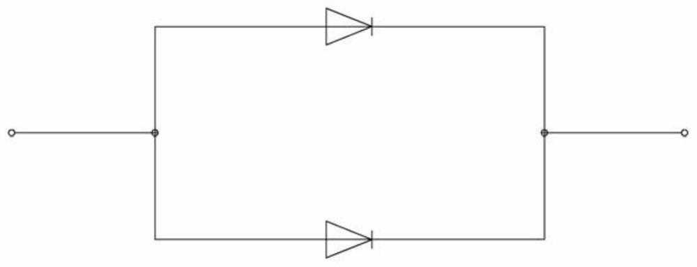
technical field [0001] The invention relates to the technical field of diodes, in particular to a high-power silicon carbide diode and a manufacturing method thereof. Background technique [0002] Silicon carbide material has the characteristics of wide band gap, high breakdown field strength, high thermal conductivity, high saturation electron migration rate and excellent physical and chemical stability, and is suitable for working in high temperature, high frequency, high power and extreme environment, so Some diodes use silicon carbide materials to replace traditional silicon materials to make silicon carbide diodes. [0003] Usually, in order to increase the power of silicon carbide diodes, two silicon carbide chips are generally connected in parallel, such as figure 1 circuit schematic shown. For this high-power silicon carbide diode, two silicon carbide chips are usually welded together on the same conductive plate, such as figure 2 The structure of the first conve...

Claims


Application Information

Patent Timeline
Patent Type & Authority Patents(China)
IPC IPC(8): H01L25/07H01L23/495H01L23/31H01L29/872H01L21/50H01L21/56H01L21/60
CPCH01L25/072H01L29/872H01L23/49562H01L23/49517H01L23/49575H01L23/3107H01L21/50H01L21/56H01L24/80
Inventor 骆宗友
Owner 东莞市佳骏电子科技有限公司
Learn More