
Device and method for preparing equivalent test piece for simulating defects of photovoltaic module

A photovoltaic module and defect technology, which is applied to the preparation device of the effective test piece and the preparation field thereof, to achieve the effect of preventing bad results and having a small volume

Active Publication Date: 2021-07-30
HARBIN UNIV OF COMMERCE
View PDF10 Cites 0 Cited by
  • Summary
  • Abstract
  • Description
  • Claims
  • Application Information

AI Technical Summary

Problems solved by technology

[0003] The present invention aims to solve the technical problem that the defects on the existing photovoltaic modules can only be studied through computer models, and provides a device and method for preparing an equivalent test piece for simulating the defects of photovoltaic modules. The device and method of the present invention can be used in Clear and clear local defects are produced on the photovoltaic unit, the position and size of local defects can be controlled, and it is an equivalent test piece for simulating ohmic shunt and weak diode effect defects

Method used


Image

  • Device and method for preparing equivalent test piece for simulating defects of photovoltaic module
  • Device and method for preparing equivalent test piece for simulating defects of photovoltaic module
  • Device and method for preparing equivalent test piece for simulating defects of photovoltaic module

Examples


Embodiment 1

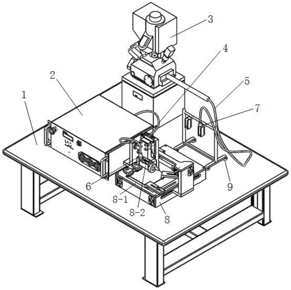
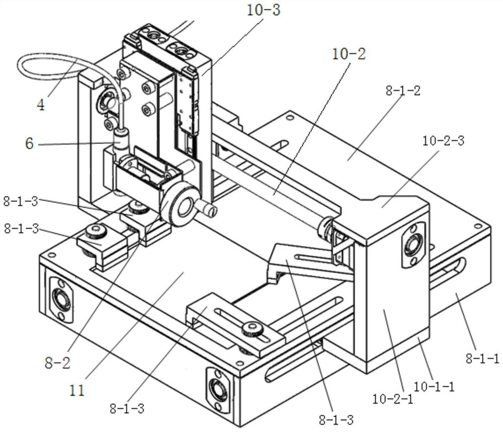
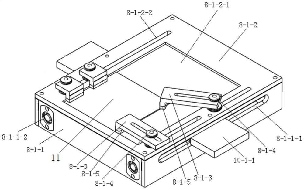
[0070] Embodiment 1: The device for preparing an equivalent test piece for simulating photovoltaic module defects in this embodiment consists of a stage 1, a femtosecond laser generator 2, a focused ion beam generator 3, a femtosecond laser fiber 4, and a focused ion beam conduction line 5. Femtosecond laser emitting head 6, focused ion beam emitting head 7, defect processing mechanism 8, object carrier 9 and three-dimensional moving device 10;

[0071] Wherein said femtosecond laser generator 2 is used for producing femtosecond laser, and femtosecond laser fiber 4 is used for conducting femtosecond laser, and femtosecond laser generator 2 is connected with femtosecond laser emitting head 6 through femtosecond laser fiber 4; The second laser passes through the femtosecond laser emitting head 7 and acts on the surface of single / polycrystalline silicon solar cells, which can produce clear local weak diode effect defects;

[0072] The focused ion beam generator 3 is used to gener...


PUM

PropertyMeasurementUnit
thicknessaaaaaaaaaa

Abstract

The invention discloses a device and a method for preparing an equivalent test piece for simulating defects of a photovoltaic module, relates to a device and a method for preparing an equivalent test piece for a defect unit of the photovoltaic module, and aims to solve the technical problem that the defects on the conventional photovoltaic module can only be researched through a computer model. The device comprises a femtosecond laser generator, a focused ion beam generator, a femtosecond laser fiber, a focused ion beam conduction line, a femtosecond laser emission head, a focused ion beam emission head, a defect processing mechanism and a carrier which are arranged on an objective table, wherein the femtosecond laser generator is connected with the femtosecond laser emission head through the femtosecond laser fiber, and the focused ion beam generator is connected with the focused ion beam emission head through the focused ion beam conduction line. The method comprises the following steps of fixing a solar cell on a defect processing mechanism, and firing the solar cell with femtosecond laser or focused ion beam to obtain an ohmic shunt or weak diode effect defect equivalent test piece. The method and the device are applied to the field of solar cells.

Description

technical field [0001] The invention relates to a preparation device and a preparation method for an equivalent test piece of a defective unit of a photovoltaic module, in particular to a preparation device and a preparation method for an equivalent test piece of a defective unit of a photovoltaic module for simulating ohmic shunt and weak diode effect. Background technique [0002] The efficient use of new energy in recent years has made photovoltaic power generation technology one of the key technologies for future renewable energy supply. Photovoltaic cells and their photovoltaic modules are rapidly developing and applied in various industries, and the development of power generation efficiency of a single photovoltaic cell has made great progress, but the difference between the power generation efficiency of a single photovoltaic cell and photovoltaic modules is There is a great distance. The reason may be that defects such as local ohmic shunt and weak diode effect of ...

Claims


Application Information

Patent Timeline
Patent Type & Authority Applications(China)
IPC IPC(8): G01N25/72H02S50/10B23K26/36
CPCG01N25/72H02S50/10B23K26/36Y02E10/50
Inventor 卜迟武刘涛赵博李锐唐庆菊
Owner HARBIN UNIV OF COMMERCE
Learn More