Device and method for processing two-dimensional nanostructure
A two-dimensional nanostructure and nanotechnology, which is applied in the field of near-field optics and nanolithography, can solve the problems that the nanostructure cannot be controlled and the size and range of the thermal field cannot be effectively controlled, and the effect of accurate manufacturing can be achieved.
- Summary
- Abstract
- Description
- Claims
- Application Information
AI Technical Summary
Problems solved by technology
Method used
Image
Examples
Embodiment 1
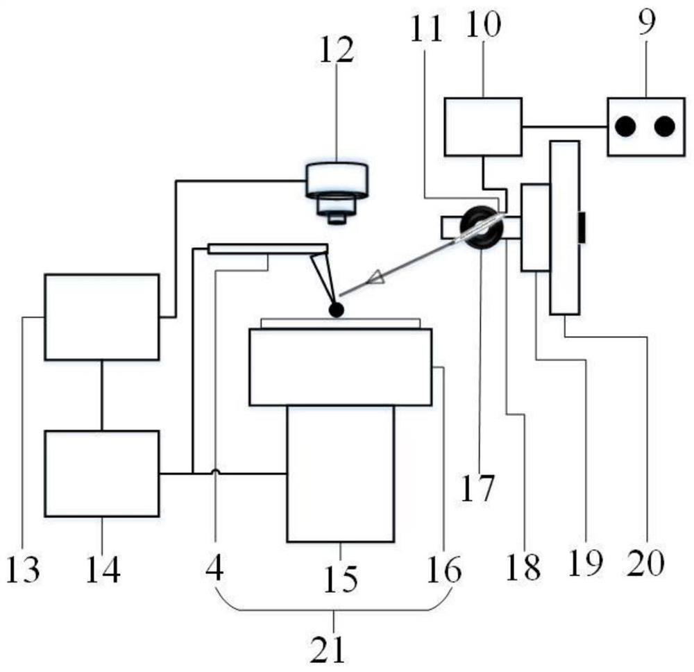
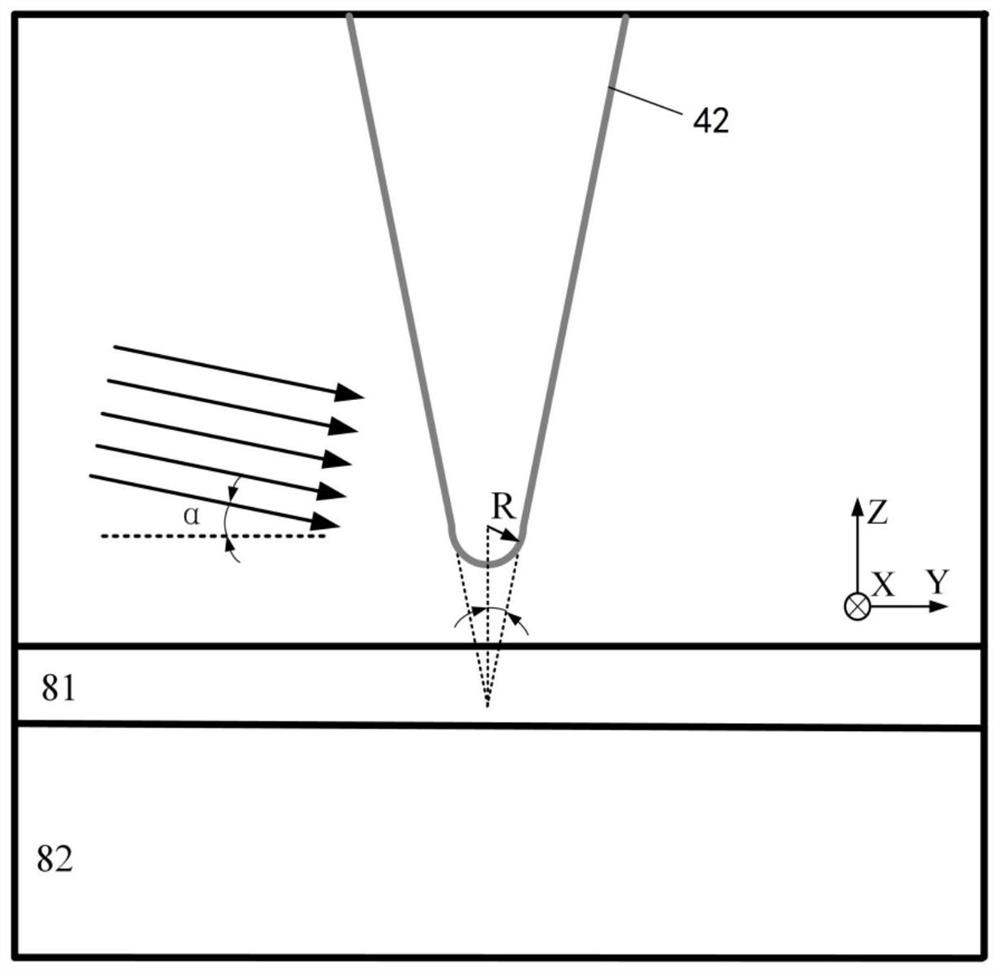
[0035] A device for processing two-dimensional nanostructures, which is realized by non-contact processing by adjusting the laser wavelength to induce controllable enhanced near-field, the device includes a fiber laser controller 9, a multi-wavelength single-mode fiber continuous laser 10, and a laser collimator 11 , CCD infrared camera 12, X-axis precision moving stage 18, Y-axis precision moving stage 19, Z-axis precision moving stage 20, 360-degree rotating stage 17, control host 14, display 13, atomic force microscope 21, said atomic force microscope 21 includes The sample stage 16 , the piezoelectric ceramic 15 and the AFM probe 4 , the AFM probe 4 includes a cantilever arm 41 and a needle tip 42 . The control host 14 is connected to the atomic force microscope 21 and the display 13. All operations are input through the display 13 and sent to the control host 14 to control the operation of the atomic force microscope 21. The piezoelectric ceramic 15 is located under the sa...
Embodiment 2
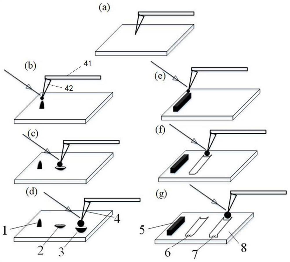
[0048] refer to figure 1 In (a)-(d), a method for processing two-dimensional nanostructures, using a multi-wavelength single-mode fiber continuous laser composite atomic force microscope probe device, by adjusting the laser output wavelength to induce a controllable enhanced near-field, to non-contact The surface of the sample is processed by means of the following steps:
[0049] Set the scanning range of the atomic force microscope 21 through the display 13 to 8um*8um, the scanning speed to 0.4 microns / second, and the graphic resolution to 512, and then use the piezoelectric ceramics 15 to drive the sample stage 16 to move upwards along the Z-axis to reach the AFM probe 4 contact, and then stop the rising of the sample stage 16, and control the piezoelectric ceramic 15 with the control host 14 to drive the sample stage 16 to move in the X / Y plane, complete the initial scanning of the processed plane, and eliminate the influence of surface impurities.
[0050] The atomic for...
Embodiment 3
[0056] The only difference between this embodiment and Embodiment 1 is that the path program adopts the nanowire path, and the laser power is set to 150 mW.
[0057] Refer to as figure 1 In (a) and (e) to (g), a method of manufacturing a two-dimensional nanostructure, using such as figure 2 The device shown is completed and includes the following steps:
[0058] S1, complete as figure 1 Empty sweep as shown in (a);
[0059] S2. Execute the nanowire path: set the laser wavelength to 532 nanometers, perform processing and scanning, and obtain such as figure 1 (e) nanowire protrusions 5 of 3nm-5nm shown;
[0060] S3. Move the sample stage 16 to another position, set the laser wavelength to 800 nanometers, continue to execute the nanowire path, and obtain such as figure 1 (f) shows the nanometer shallow groove 6, move the sample stage to another position again, set the laser wavelength to 1064 nanometers, execute the nanowire path, and obtain the following image after proces...
PUM
| Property | Measurement | Unit |
|---|---|---|
| thickness | aaaaa | aaaaa |
Abstract
Description
Claims
Application Information
 - R&D
- Intellectual Property
- Life Sciences
- Materials
- Tech Scout
- Unparalleled Data Quality
- Higher Quality Content
- 60% Fewer Hallucinations
Browse by: Latest US Patents, China's latest patents, Technical Efficacy Thesaurus, Application Domain, Technology Topic, Popular Technical Reports.
© 2025 PatSnap. All rights reserved.Legal|Privacy policy|Modern Slavery Act Transparency Statement|Sitemap|About US| Contact US: help@patsnap.com


