Manufacturing process of semi-floating gate memory and semi-floating gate memory

A manufacturing process, semi-floating gate technology, applied in the direction of semiconductor devices, electrical solid state devices, electrical components, etc., can solve the problems of increasing the integration density that have not been mentioned, so as to increase the integration density and increase the charge writing speed , which favors the ever-shrinking effect

Active Publication Date: 2021-07-23
FUDAN UNIV +1
View PDF14 Cites 0 Cited by
  • Summary
  • Abstract
  • Description
  • Claims
  • Application Information

AI Technical Summary

Problems solved by technology

However, there is no mention of a semi-floating gate memory that can increase the integration density, increase the charge writing speed, and at the same time be able to produce in a large area and be compatible with existing manufacturing processes

Method used


Image

  • Manufacturing process of semi-floating gate memory and semi-floating gate memory
  • Manufacturing process of semi-floating gate memory and semi-floating gate memory
  • Manufacturing process of semi-floating gate memory and semi-floating gate memory

Examples


Embodiment Construction

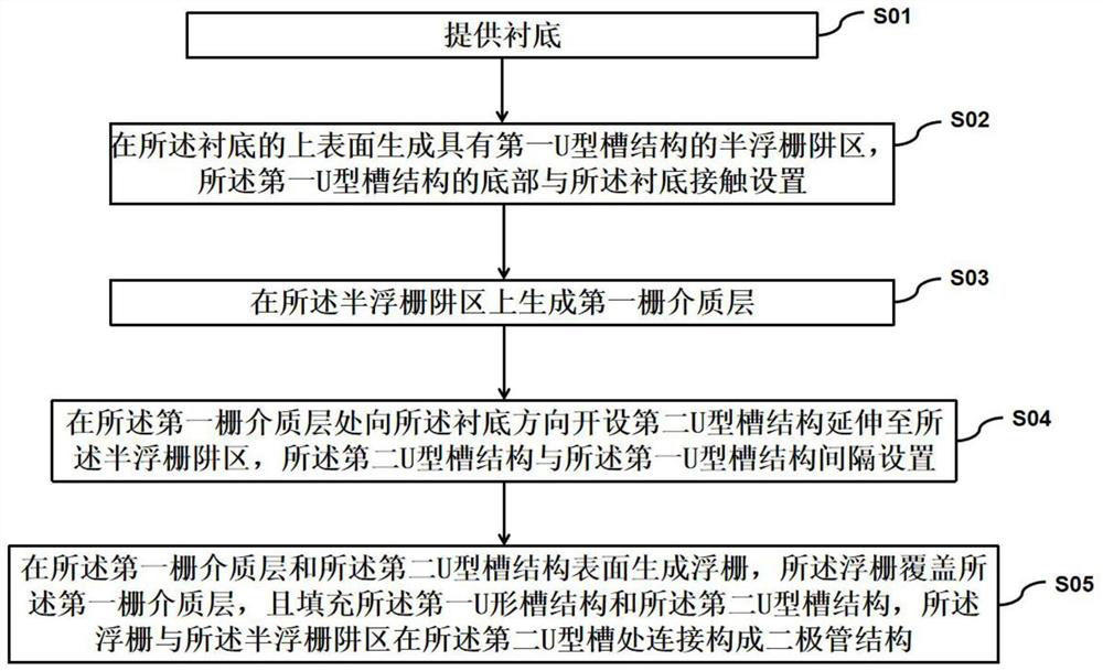
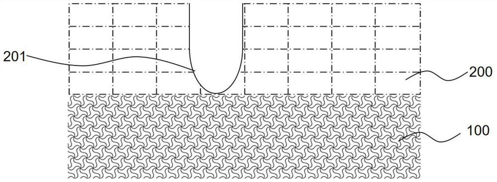
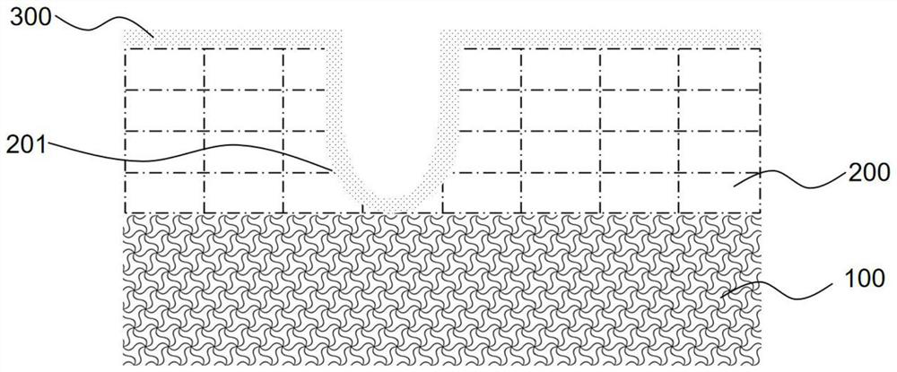
[0057] In order to make the purpose, technical solutions and advantages of the present invention clearer, the technical solutions in the embodiments of the present invention will be clearly and completely described below in conjunction with the accompanying drawings of the present invention. Obviously, the described embodiments are part of the present invention Examples, not all examples. Based on the embodiments of the present invention, all other embodiments obtained by persons of ordinary skill in the art without creative efforts fall within the protection scope of the present invention. Unless otherwise defined, the technical terms or scientific terms used herein shall have the usual meanings understood by those skilled in the art to which the present invention belongs. As used herein, "comprising" and similar words mean that the elements or items appearing before the word include the elements or items listed after the word and their equivalents, without excluding other el...


PUM


Abstract

The invention provides a manufacturing process of a semi-floating gate memory. The manufacturing process comprises the following steps: providing a substrate; generating a semi-floating gate well region with a first U-shaped groove structure on the upper surface of the substrate, wherein the bottom of the first U-shaped groove structure is in contact with the substrate; generating a first gate dielectric layer on the semi-floating gate well region; forming a second U-shaped groove structure in the first gate dielectric layer in the direction of the substrate and extending to the semi-floating gate well region, wherein the second U-shaped groove structure and the first U-shaped groove structure are arranged at an interval; and generating a floating gate on the surfaces of the first gate dielectric layer and the second U-shaped groove structure, wherein the floating gate covers the first gate dielectric layer and fills the first U-shaped groove structure and the second U-shaped groove structure, and the floating gate and the semi-floating gate well region are connected at the second U-shaped groove to form a diode structure. According to the invention, the channel region and the diode region of the semi-floating gate transistor are formed by constructing the U-shaped groove structure; and integration density is increased and a charge writing speed is increased too, meanwhile, large-area production can be realized, and the process is compatible with the existing manufacturing process. In addition, the invention also provides the semi-floating gate memory.

Description

technical field [0001] The invention relates to the technical field of semiconductor storage, in particular to a manufacturing process of a half-floating gate memory and the half-floating gate memory. Background technique [0002] Today's mainstream storage technology is divided into two categories: volatile storage technology and non-volatile storage technology. [0003] Among them, the volatile storage technologies are mainly Static Random-Access Memory (SRAM) and Dynamic Random Access Memory (DRAM). Volatile memory has a write speed of nanometers, but its data retention capability is only milliseconds, making it only used in limited storage areas such as caches. [0004] For non-volatile storage technologies, such as flash memory technology, its data retention capability can reach 10 years, but relatively slow write operations greatly limit its application in the cache field. Therefore, in this context, a semi-floating gate memory based on two-dimensional semiconductor ...

Claims


Application Information

Patent Timeline
Patent Type & Authority Applications(China)
IPC IPC(8): H01L27/11521H01L27/11526H01L27/11531
CPCH10B41/30H10B41/40H10B41/42
Inventor 陈琳朱宝孙清清张卫
Owner FUDAN UNIV
Why Eureka
Try Eureka