OLED display panel, preparation method thereof and display device
A display panel and display area technology, which is applied in semiconductor/solid-state device manufacturing, semiconductor devices, electrical components, etc., can solve the problems of OLED display panel poor transmittance, unfavorable camera shooting effect under the screen, etc., and achieve enhanced overall transmittance efficiency, avoid membrane layer separation, and improve the effect of adsorption
- Summary
- Abstract
- Description
- Claims
- Application Information
AI Technical Summary
Problems solved by technology
Method used
Image
Examples
Embodiment 1
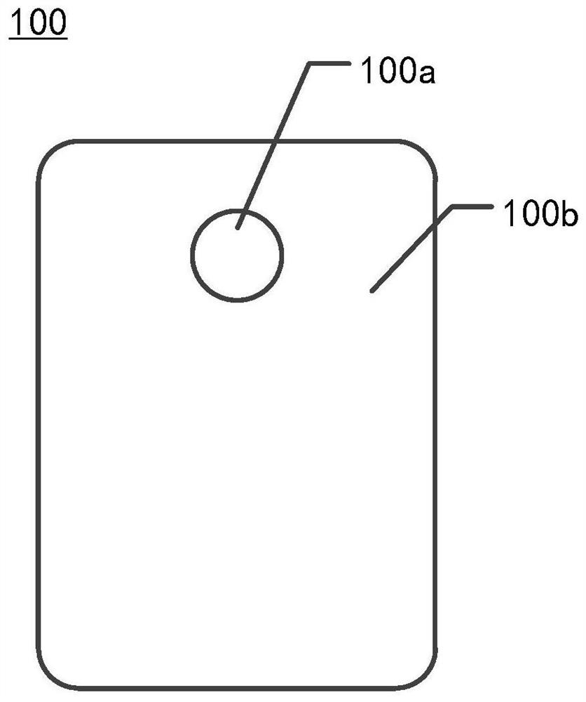
[0053] figure 1 A plan view of the OLED display panel provided in Embodiment 1 of the present application.
[0054] like figure 1 As shown, the present embodiment provides an OLED display panel 100, which includes a first display area 100a and a second display area 100b surrounding the first display area 100a.
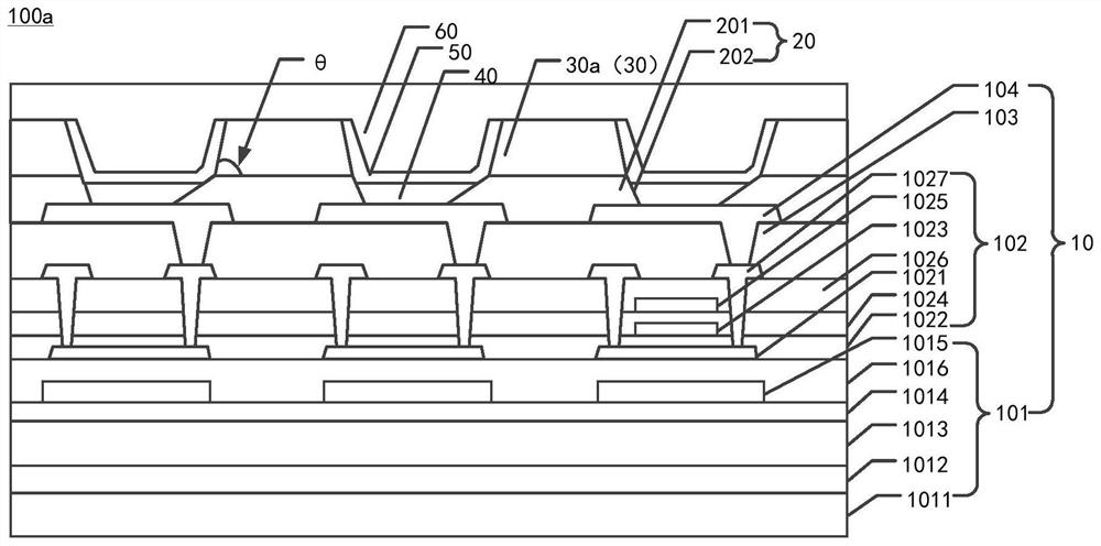
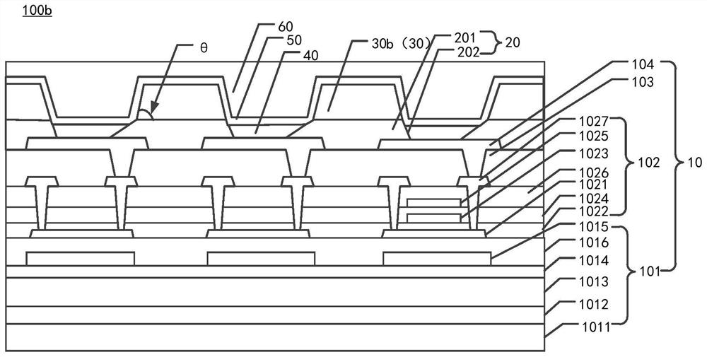
[0055] figure 2 is a cross-sectional view of the first display area provided by Embodiment 1 of the present application; image 3 is a cross-sectional view of the second display area provided by Embodiment 1 of the present application.
[0056] like Figure 2-Figure 3 As shown, the OLED display panel 100 further includes a substrate 10 , a pixel definition layer 20 , a spacer layer 30 , a light emitting layer 40 , a cathode 50 and an encapsulation layer 60 .
[0057] The substrate 10 extends from the first display area 100a to the second display area 100b.
[0058] Specifically, the substrate 10 includes a substrate layer 101 , a thin film transistor layer 102 ,...
Embodiment 2
[0117] This embodiment provides an OLED display panel, a manufacturing method thereof, and a display device, including most of the technical solutions of Embodiment 1, the difference being that the spacer layer is only disposed in the first display region.
[0118] Figure 11 A cross-sectional view of the OLED display panel provided in Example 2 of the present application.
[0119] Specifically, such as Figure 11 As shown, the spacer layer 30 has a first spacer structure 30a, and the first spacer structure 30a is correspondingly disposed on the isolation structure 201 of the first display region 100a. The light emitting layer 40 is disposed in the pixel openings 202 of the first display area 100a and the second display area 100b. The cathode 50 is disposed on the light emitting layer 40 of the first display area 100a and the second display area 100b. In the first display area 100a, a luminescent layer 40 is located between two adjacent first spacer structures 30a; the cath...
Embodiment 3
[0122] This embodiment provides an OLED display panel, a manufacturing method thereof, and a display device, including all the technical solutions of Embodiment 1 or Embodiment 2, the difference being that the spacer layer is provided with a slot.
[0123] Figure 12 A cross-sectional view of the first display area provided for Embodiment 3 of the present application; Figure 13 is a cross-sectional view of the second display area provided by Embodiment 3 of the present application.
[0124] like Figure 12-Figure 13 As shown, this embodiment provides an OLED display panel, and the first spacer structure 30 a and the second spacer structure 30 b each have a locking groove 301 . The encapsulation layer 60 is disposed on the cathode 50 and disposed in the slot 301 , wherein the encapsulation layer 60 forms an engaging portion 601 in the slot.
[0125] Specifically, in the first display area 100a, the encapsulation layer 60 is provided on the upper surface of the cathode 50 an...
PUM
| Property | Measurement | Unit |
|---|---|---|
| Angle | aaaaa | aaaaa |
| Thickness | aaaaa | aaaaa |
| Thickness | aaaaa | aaaaa |
Abstract
Description
Claims
Application Information
 - R&D
- Intellectual Property
- Life Sciences
- Materials
- Tech Scout
- Unparalleled Data Quality
- Higher Quality Content
- 60% Fewer Hallucinations
Browse by: Latest US Patents, China's latest patents, Technical Efficacy Thesaurus, Application Domain, Technology Topic, Popular Technical Reports.
© 2025 PatSnap. All rights reserved.Legal|Privacy policy|Modern Slavery Act Transparency Statement|Sitemap|About US| Contact US: help@patsnap.com


