Fabrication method and fabric of silk outlet hole, integrated fiber of optoelectronic chip

A technology for optoelectronic chips and manufacturing methods, applied in fabrics, braids, fiber processing, etc., can solve the problems of limited fiber length, complex preparation process, complex fiber devices, etc., and achieve excellent performance, high luminous intensity, and low power consumption Effect

Active Publication Date: 2022-08-05
HUAZHONG UNIV OF SCI & TECH
View PDF7 Cites 0 Cited by
  • Summary
  • Abstract
  • Description
  • Claims
  • Application Information

AI Technical Summary

Problems solved by technology

Because this method can deposit different materials in sequence, it can realize a variety of in-fiber devices, such as PN junctions, Schottky junctions, PIN junctions, ohmic contacts, etc. in fibers, but this process has certain limitations. The fiber length is limited, only centimeter to millimeter-scale fibers can be realized, and it is only suitable for materials that can be synthesized in the gas phase within the fiber, which has great restrictions on the materials used
[0006] The integration of functional fiber devices by doping materials with different electrical and optical properties in fibers is complex and limited, because a variety of materials are required to realize complex functions in fibers, including crystalline semiconductor materials, high-melting point alloys, Films, thermosetting polymers, etc., and these materials are often unable to achieve co-drawing with fiber materials. Due to the limitations of these materials and the requirements of micro-scale size control for micro-electronic devices, this method is used to fully integrate micro-electronic devices into fiber is not feasible
[0007] Chinese invention patent CN107564730A discloses a fluorescent fiber-shaped supercapacitor and its preparation. Oriented carbon nanotube fibers uniformly loaded with fluorescent components are used as electrodes, and the surfaces of the two fiber electrodes are uniformly coated with gel electrolyte and then intertwined to form a winding structure. Fluorescent supercapacitor fibers, but the preparation process is more complicated, and an external coating needs to be added
Chinese invention patent CN110227208A discloses a flexible fiber electrode coated with polyetheretherketone coating, which adopts the method of thermal softening and drawing, and performs co-drawing of polyetheretherketone preform and flexible filamentary conductive material to obtain a flexible fiber electrode. The flexible fiber electrode with polyether ether ketone as the core layer and polyether ether ketone as the cladding has the limitation that more other materials with thermal or electrical properties need to be added to achieve more complex functions, and the requirements for materials There will be more and more

Method used


Image

  • Fabrication method and fabric of silk outlet hole, integrated fiber of optoelectronic chip
  • Fabrication method and fabric of silk outlet hole, integrated fiber of optoelectronic chip
  • Fabrication method and fabric of silk outlet hole, integrated fiber of optoelectronic chip

Examples


Embodiment 1

[0092] In the first embodiment of the present invention, a red light emitting fiber is prepared by a wet spinning method.

[0093] The fibrous base material selects PC particles with a diameter of about 3 mm. The optoelectronic chip selects a light-emitting diode, specifically, an AlGaInP red light-emitting diode from ES-SABRPN14D of EPISTAR Company in Taiwan, China, with a wavelength of 660 nm, a chip size of 340 μm × 340 μm × 170 μm, and electrical contacts on opposite sides of the chip. The lead wire is a tungsten wire with a wire diameter of 50 μm.

[0094] Preparation of spinning substrate: 40 g of PC particles were dried in a vacuum oven at 60 °C for 24 hours, taken out, and then added with 350 mL of dimethylformamide solvent, and stirred in the dark until the particles were completely dissolved, to obtain a certain viscosity and good reproducibility. Spinnable spinning substrate.

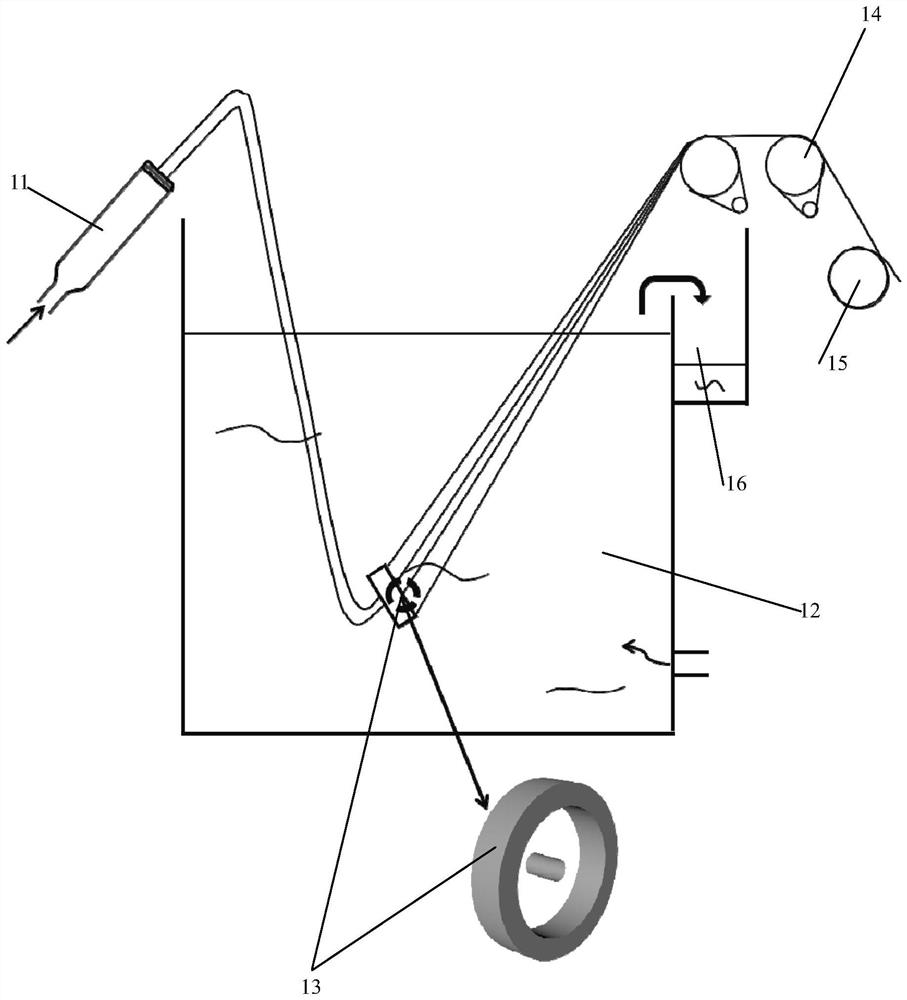
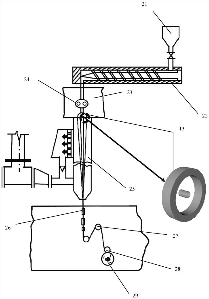
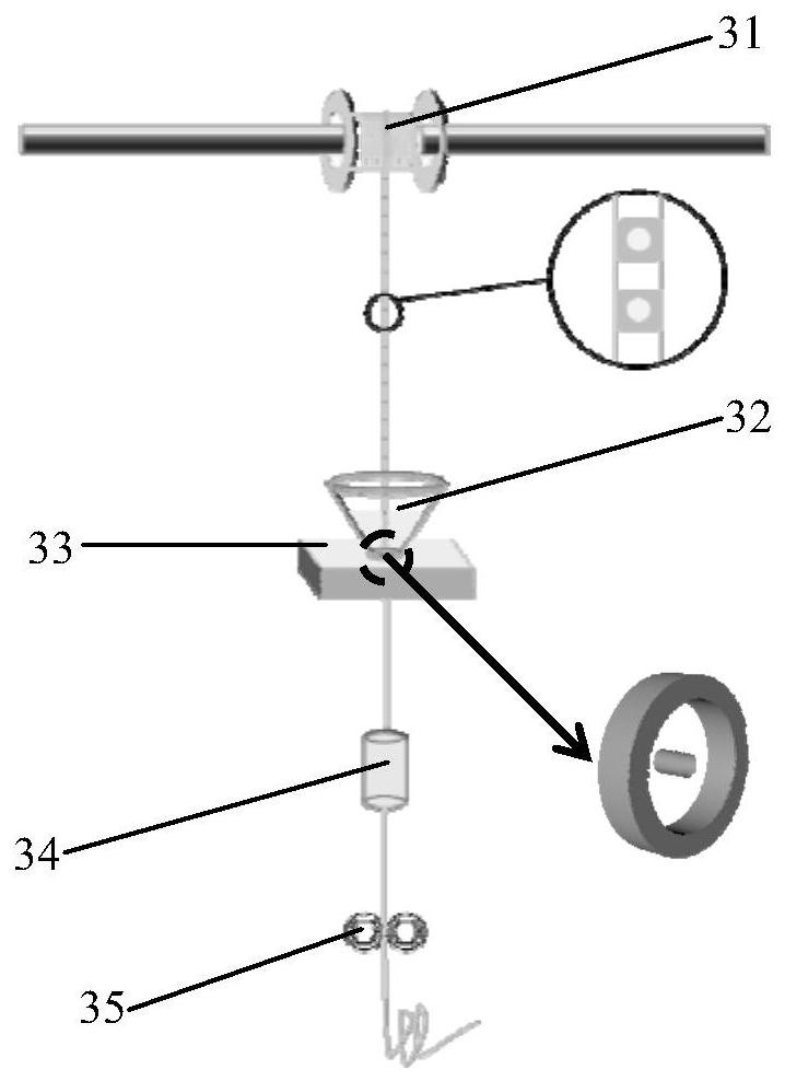
[0095] Arrange a plurality of red light-emitting diodes at intervals along one directio...

Embodiment 2

[0098] In the second embodiment of the present invention, the red light emitting hydrogel fiber is prepared by wet spinning method.

[0099] The fibrous base material selects sodium alginate particles with a diameter of 2 mm. The light-emitting diode is an AlGaInP red light-emitting diode of ES-SABRPN14D from EPISTAR, China, with a wavelength of 660 nm, a chip area of ​​340 μm × 340 μm × 170 μm, and electrical contacts on opposite sides of the chip. The lead wire is a tungsten wire with a wire diameter of 50 μm.

[0100] Preparation of spinning substrate: drying 35 g of sodium alginate particles in a vacuum oven at 60°C for 24 hours, taking out and adding 300 mL of cold water, stirring until the particles are completely dissolved, to obtain a spinning substrate with a certain viscosity and good spinnability .

[0101] Arrange a plurality of red light-emitting diodes at intervals along one direction, in a row, use a wire bonding machine, and follow the Figure 4 In the metho...

Embodiment 3

[0104]In the third embodiment of the present invention, a red light emitting fiber is prepared by a melt spinning method.

[0105] The fibrous base material selects PC particles with a diameter of about 3 mm. The optoelectronic chip selects light-emitting diodes, specifically the AlGaInP red light-emitting diodes from ES-SABRPN14D of EPISTAR Company in Taiwan, China, with a wavelength of 660nm, a chip area of ​​340μm × 340μm × 170μm, and electrical contacts on opposite sides of the chip. The lead wire is a tungsten wire with a wire diameter of 50 μm.

[0106] Arrange a plurality of red light-emitting diodes at intervals along one direction, in a row, use a wire bonding machine, according to Figure 4 In the method of , two tungsten wires with a wire diameter of 50 μm are welded to the two pins of the red light-emitting diode respectively to form a combination of photoelectric chips and leads. Each of the red light emitting diodes is separated by 30mm, and a row of 500 red li...


PUM

PropertyMeasurementUnit
viscosityaaaaaaaaaa
thicknessaaaaaaaaaa
diameteraaaaaaaaaa

Abstract

A method and fabric for producing a fiber exit hole and an integrated fiber of an optoelectronic chip, the spinning base material comprising a fiber base material is prepared; the lead wire is electrically connected with the pin of the optoelectronic chip to form at least one group of electrically connected optoelectronic chip and the lead wire. combination; feeding the combination of the at least one group of electrically connected optoelectronic chips and leads into the channel in the above-mentioned exit hole, and feeding the spinning substrate into the exit hole by a spinning method; The spinning hole ejects the primary fibers including the electrically connected leads, the optoelectronic chip and the spinning base material, and the encapsulation of the electrically connected optoelectronic chips and the leads is realized during the ejection process; The photoelectric chip integrated fiber is obtained after the primary fiber is formed and processed. The invention combines optoelectronic chip integrated fibers with textiles, which not only makes textiles "smart", but also maintains the original softness and comfort of textiles, can better fit the skin, and can be applied to the field of smart wearables .

Description

technical field [0001] The present invention relates to a fiber manufacturing method and corresponding structure and fabric, in particular to a manufacturing method of optoelectronic chip integrated fiber and corresponding fiber products. Background technique [0002] With the development of composite materials and people's demand for intelligent life, and the boom in the field of functional fibers in recent years, various functional fibers have been manufactured, such as conductive fibers, thermally conductive fibers, and magnetron fibers. In addition, scientists also combine it with textiles in the field of smart wearables to achieve various functions such as communication, physiological monitoring, temperature regulation, and flexible lighting. [0003] Traditional wearable devices are produced on hard substrate boards, and functional devices are attached to the surface of the fabric, which will affect the wearing comfort of the user, while building fiber-based devices an...

Claims


Application Information

Patent Timeline
Patent Type & Authority Patents(China)
IPC IPC(8): D01D5/253D01D5/06D01D5/08D01D5/00D02G3/44D03D15/283D04B1/16D04B21/00D04C1/02H01L33/48H01L33/54H01L33/62
CPCD01D5/253D01D5/06D01D5/08D01D5/00D02G3/441D04B1/16D04B21/00D04C1/02H01L33/48H01L33/54H01L33/62H01L2933/0033H01L2933/005H01L2933/0066
Inventor 陶光明赵淑雅李攀
Owner HUAZHONG UNIV OF SCI & TECH
Why Eureka
Try Eureka