
Solar cell and manufacturing method thereof

A technology of solar cells and manufacturing methods, which is applied to circuits, electrical components, photovoltaic power generation, etc., and can solve problems such as unsatisfactory processing effects, winding and plating of doped polysilicon layers, and degradation of battery performance.

Active Publication Date: 2021-06-01
TAIZHOU LERRISOLAR TECH CO LTD
View PDF5 Cites 7 Cited by
  • Summary
  • Abstract
  • Description
  • Claims
  • Application Information

AI Technical Summary

Problems solved by technology

[0003] When the doped polysilicon layer included in the passivation contact structure is connected to the doped layer on the side and front of the silicon wafer, it is prone to leakage problems, which greatly reduces battery performance
Even if the doped polysilicon layer is removed in the subsequent process, the doped layer on the side of the silicon wafer cannot be removed
Moreover, compared with amorphous silicon, polysilicon is difficult to remove, and there is likely to be a residual doped polysilicon layer around the plating, causing leakage problems
[0004] In the prior art, silicon wafers are also subjected to edge isolation treatment, but the treatment process is complicated and the treatment effect is not ideal

Method used


Image

  • Solar cell and manufacturing method thereof
  • Solar cell and manufacturing method thereof
  • Solar cell and manufacturing method thereof

Examples


Embodiment Construction

[0035] In order to clearly describe the technical solutions of the embodiments of the present invention, in the embodiments of the present invention, words such as "first" and "second" are used to distinguish the same or similar items with basically the same function and effect. Those skilled in the art can understand that words such as "first" and "second" do not limit the number and execution order, and words such as "first" and "second" do not necessarily limit the difference.

[0036] It should be noted that, in the present invention, words such as "exemplary" or "for example" are used as examples, illustrations or illustrations. Any embodiment or design described herein as "exemplary" or "for example" should not be construed as being preferred or advantageous over other embodiments or designs. Rather, the use of words such as "exemplary" or "such as" is intended to present related concepts in a concrete manner.

[0037]In the present invention, "at least one" means one o...


PUM

PropertyMeasurementUnit
Widthaaaaaaaaaa

Abstract

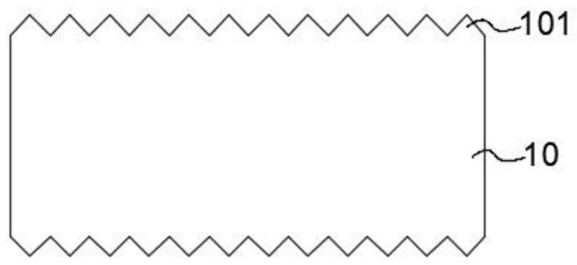
The invention discloses a solar cell and a manufacturing method thereof, relates to the technical field of photovoltaics, and aims to conveniently form an isolation part and reduce the probability of electric leakage of the solar cell. The manufacturing method of the solar cell comprises the following steps of: providing a silicon substrate; forming a tunneling layer on the back surface of the silicon substrate; forming an amorphous silicon layer on the tunneling layer; processing the first part of the amorphous silicon layer to form a doped polycrystalline silicon region and an amorphous silicon region surrounding the doped polycrystalline silicon region; removing the amorphous silicon region and the tunneling layer covered by the amorphous silicon region; and acquiring a passivation contact structure and an isolation part surrounding the passivation contact structure. The solar cell and the manufacturing method thereof provided by the invention are used for solar cell manufacturing.

Description

technical field [0001] The invention relates to the field of photovoltaic technology, in particular to a solar cell and a manufacturing method thereof. Background technique [0002] With the development of solar photovoltaic technology, tunneling passivation contact (TOPCon) cells have better passivation contact properties and have gradually become typical high-efficiency solar cells. In the process of making TOPCon cells, a layer of intrinsic amorphous silicon is usually grown on the tunneling layer on the back of the silicon wafer, and then the intrinsic amorphous silicon is doped by thermal diffusion to make the intrinsic amorphous silicon into a doped polysilicon layer to form a passivation contact structure. During the thermal diffusion process, doping impurities will not only enter the intrinsic amorphous silicon layer and the surrounding amorphous silicon layer, but also enter the back and side surfaces of the silicon wafer to form a doped layer. [0003] When the d...

Claims


Application Information

Patent Timeline
IPC IPC(8): H01L31/18H01L31/06
CPCH01L31/1868H01L31/1804H01L31/06Y02P70/50Y02E10/547
Inventor 童洪波张洪超李华刘继宇
Owner TAIZHOU LERRISOLAR TECH CO LTD
Learn More