A cleaning device for wafers

A technology for cleaning devices and wafers, which is applied in the direction of cleaning methods using liquids, cleaning methods using tools, cleaning methods and utensils, etc., which can solve the problems of low cleaning agent use efficiency, time-consuming and labor-intensive use, and improve kinetic energy utilization. , Improve the cleaning effect and avoid the effect of empty spray

Active Publication Date: 2021-08-27
JIANGSU ASIA ELECTRONICS TECH CO LTD
View PDF6 Cites 2 Cited by
  • Summary
  • Abstract
  • Description
  • Claims
  • Application Information

AI Technical Summary

Problems solved by technology

[0003] In the current wafer cleaning, most of them use the cleaning tank ultrasonic cleaning method, although this method can make the wafer clean, and after cleaning, it needs to be removed, drained, wiped, and dried, which is time-consuming and laborious. At the same time, the use of cleaning agents not efficient

Method used


Image

  • A cleaning device for wafers
  • A cleaning device for wafers
  • A cleaning device for wafers

Examples


Embodiment 1

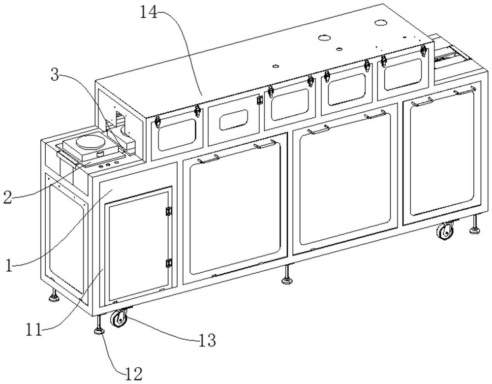
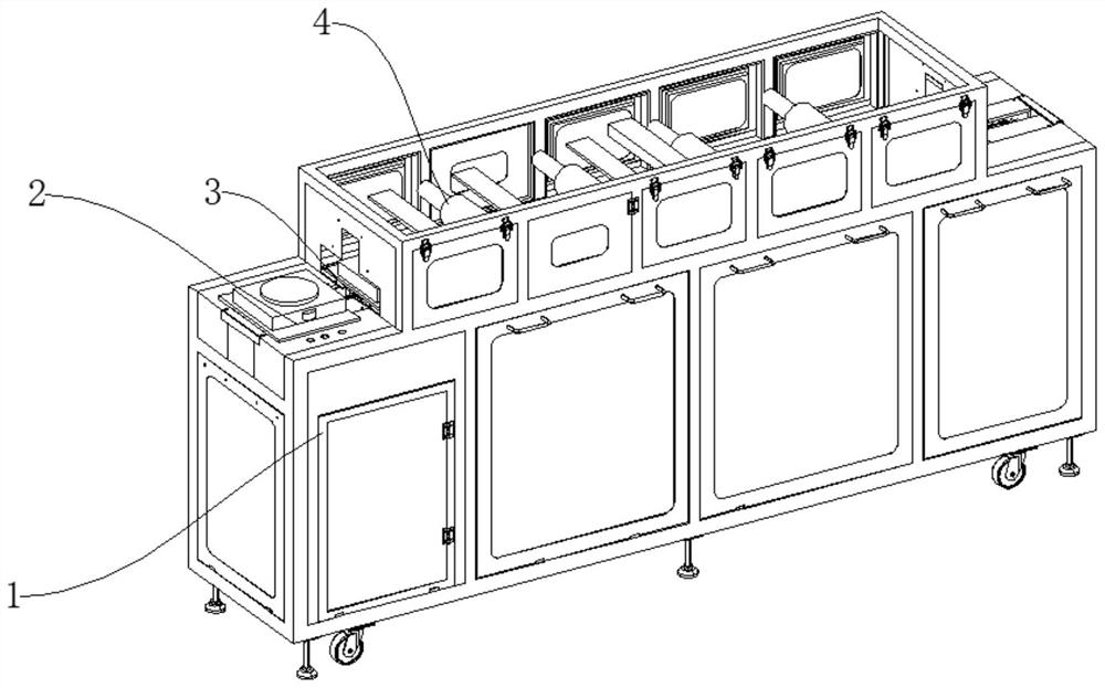
[0048] like Figure 1-Figure 9 As shown, a cleaning device for wafers includes a protection mechanism 1, a fixing mechanism 2, a conveying mechanism 3, and a cleaning mechanism 4. The protection mechanism 1 is provided with a conveying mechanism 3, and the upper end of the conveying mechanism 3 is connected with a fixing mechanism 2, A cleaning mechanism 4 is arranged on the upper side of the fixing mechanism 2, the cleaning mechanisms 4 are connected by a linkage mechanism 5, and the power ends of the cleaning mechanism 4 and the transmission mechanism 3 are connected to the power mechanism 6;

[0049] The protection mechanism 1 includes a circulating water tank 11, a first fixed seat 12, a universal wheel 13, and a cleaning box 14. The upper end of the circulating water tank 11 is provided with a cleaning box 14, the circulating water tank 11 is provided with a water tank and a circulating pump, and the lower end of the circulating water tank 11 is provided with a water tank ...

Embodiment 2

[0056] like Figure 10 The difference between this embodiment and Embodiment 1 is:

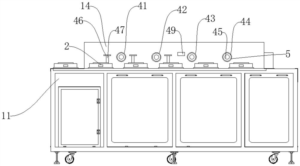
[0057] The linkage mechanism 5 includes a driving bevel gear 511, a driven bevel gear 512, a worm 513, and a worm wheel 514. The driving bevel gear 511 is connected to the first central shaft 45, the lower end of the driving bevel gear 511 meshes with the driven bevel gear 512, and the driven bevel gear 512 A worm 513 is connected to the worm, and three worm gears 514 are engaged with the worm 513. When multiple central shafts 45 are required to rotate, the servo motor 61 transmits power to the first central shaft 45 through the first sprocket group 62, and then passes The cooperation of the driving bevel gear 511 and the driven bevel gear 512 transmits the power to the worm 513 , and the subsequent central shaft 45 is rotated by the cooperation of the worm 513 and the worm wheel 514 .

[0058] A method for using a cleaning device for wafers, comprising the following steps:

[0059] a) Plac...


PUM


Abstract

The invention discloses a cleaning device for wafers, comprising a protection mechanism, a fixing mechanism, a conveying mechanism and a cleaning mechanism, the protection mechanism is provided with the conveying mechanism, and the upper end of the conveying mechanism is connected with the fixing mechanism The cleaning mechanism is arranged on the upper side of the fixing mechanism, the cleaning mechanisms are connected by a linkage mechanism, and the cleaning mechanism and the power end of the transmission mechanism are both connected to the power mechanism. The rack of the present invention functions as a matching gear, so that the wafer rotates during cleaning, and the utilization rate of kinetic energy is improved by using the multi-stage linkage effect. Press the elastic valve for water spray cleaning, and at the same time avoid the empty spray of the detergent, so as to improve the use efficiency of the detergent.

Description

technical field [0001] The invention relates to the field of wafer processing, in particular to a cleaning device for wafers Background technique [0002] Wafer refers to the silicon wafer used to make silicon semiconductor circuits, and its raw material is silicon. High-purity polysilicon is dissolved and mixed with silicon crystal seeds, which are then slowly pulled out to form cylindrical monocrystalline silicon. The silicon ingot is ground, polished and sliced ​​to form a silicon wafer, that is, a wafer. At present, domestic wafer production lines are mainly 8 inches and 12 inches. [0003] In the current wafer cleaning, most of them use the cleaning tank ultrasonic cleaning method, although this method can make the wafer clean, and after cleaning, it needs to be removed and drained, wiped, and dried, which is time-consuming and laborious, and the use of detergents Not very efficient either. SUMMARY OF THE INVENTION [0004] The purpose of the present invention is ...

Claims


Application Information

Patent Timeline
Patent Type & Authority Patents(China)
IPC IPC(8): H01L21/67B08B3/02B08B1/02B08B1/00B08B13/00
CPCB08B1/002B08B1/02B08B3/022B08B13/00H01L21/67046H01L21/67051
Inventor 钱诚李刚周兴江
Owner JIANGSU ASIA ELECTRONICS TECH CO LTD
Why Eureka
Try Eureka