Hot pressing sintering clamp for chip packaging and chip packaging method

A technology of hot pressing sintering and chip packaging, which is applied in sustainable manufacturing/processing, electrical components, climate sustainability, etc. It can solve the problems of large parallelism error, solder melting, uneven density, etc., and achieve pressure , to ensure uniformity, to ensure the effect of verticality

Active Publication Date: 2021-05-11
BEIHANG UNIV
View PDF6 Cites 1 Cited by
  • Summary
  • Abstract
  • Description
  • Claims
  • Application Information

AI Technical Summary

Problems solved by technology

When the traditional solder is packaged, the solder melts without pressure, so it cannot meet the hot-press sintering of the new solder
[0004] At present, there are hot-pressing sintering equipment for nano-solder paste packaging. The heating plate is pressurized mainly by the up and down movement of the screw mechanism. The parallelism of the plane in contact with the packaged device on the flat plate cannot be accurately guaranteed, or after a period of time, the parallelism error is relatively large, resulting in uneven thickness and uneven density of the sintered layer after pressure sintering, and some parts cannot be welded. Happening
In addition, when there are other structures on the chip substrate such as leads, wires, etc., the pressurization fixture of the current flat panel is not suitable
[0005] At present, the hot pressing sintering machine on the market mainly adopts the method of motor pressurization, hydraulic pressure or cylinder pressurization. The accuracy of the pressurization mechanism can only be guaranteed by the precision of processing and assembly, and the parallelism of the pressurization mechanism cannot be guaranteed after long-term use.

Method used


Image

  • Hot pressing sintering clamp for chip packaging and chip packaging method
  • Hot pressing sintering clamp for chip packaging and chip packaging method
  • Hot pressing sintering clamp for chip packaging and chip packaging method

Examples


Embodiment Construction

[0034] The following will clearly and completely describe the technical solutions in the embodiments of the present invention with reference to the accompanying drawings in the embodiments of the present invention. Obviously, the described embodiments are only some, not all, embodiments of the present invention. Based on the embodiments of the present invention, all other embodiments obtained by persons of ordinary skill in the art without making creative efforts belong to the protection scope of the present invention.

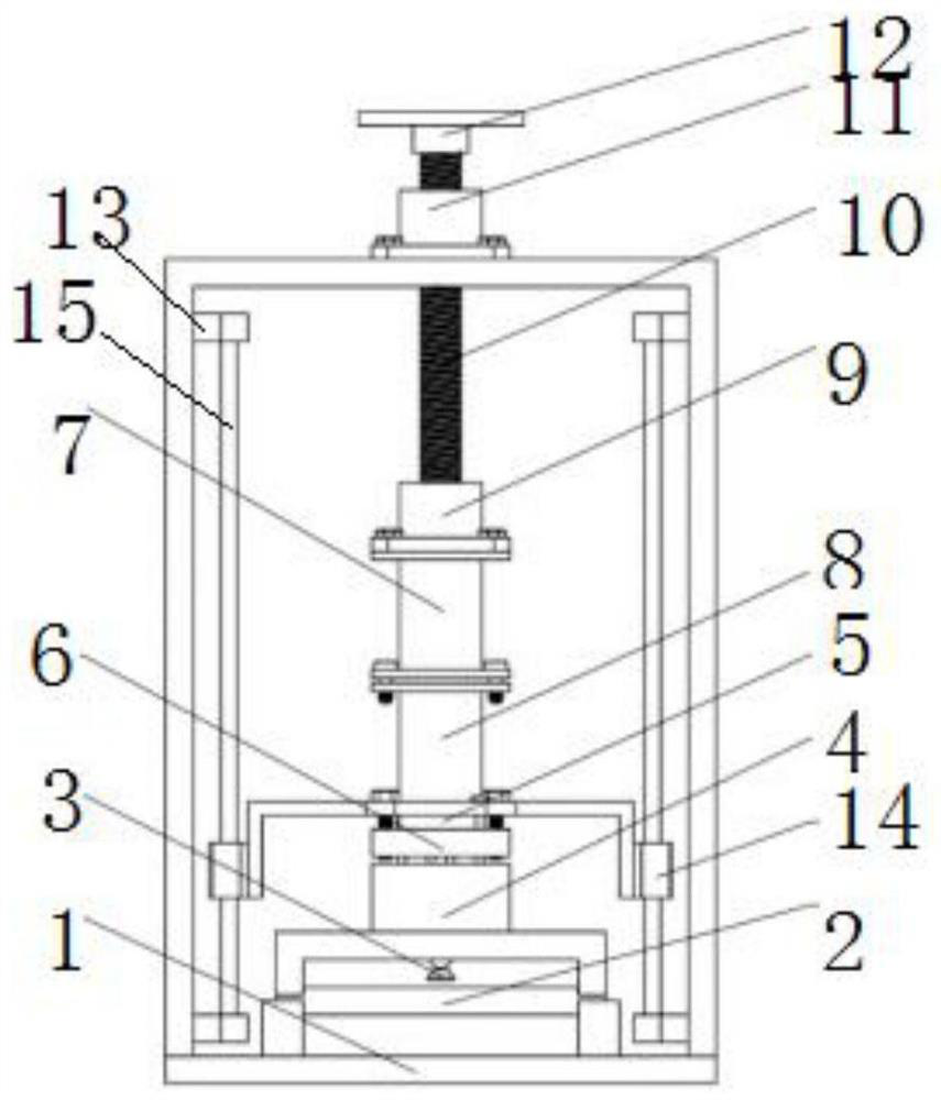
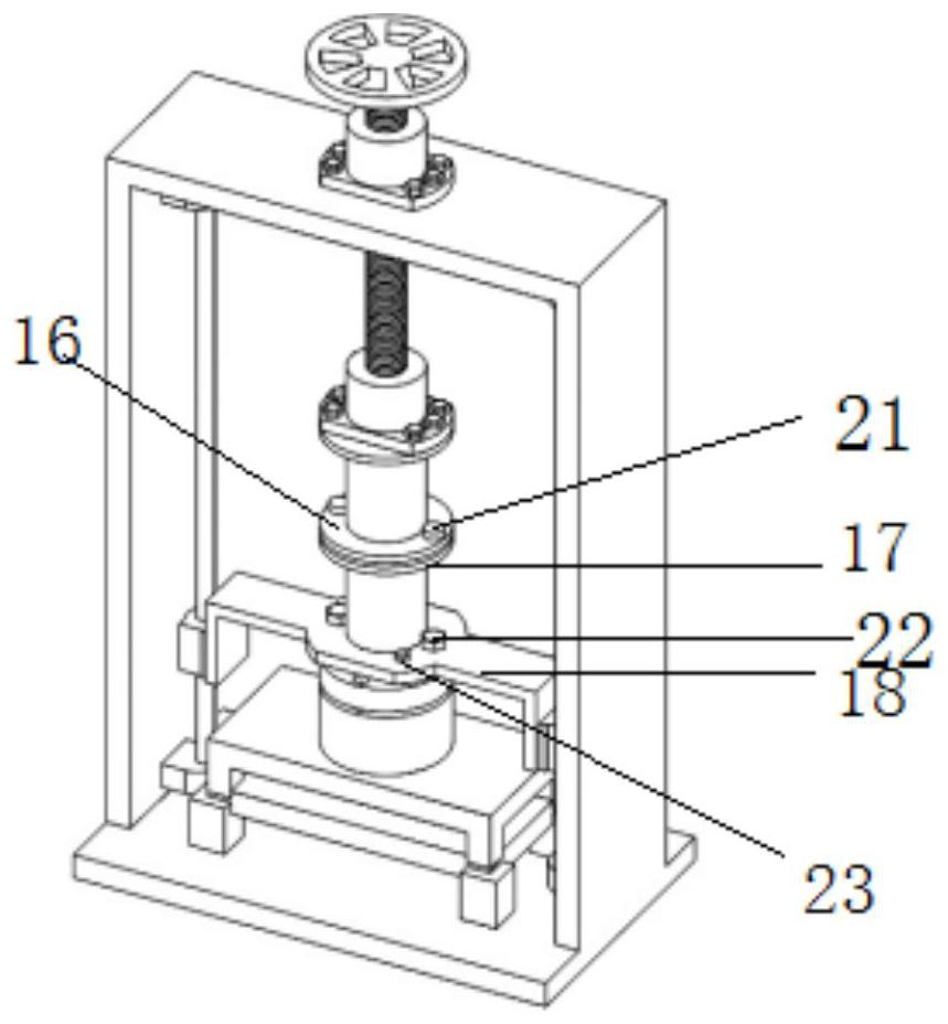
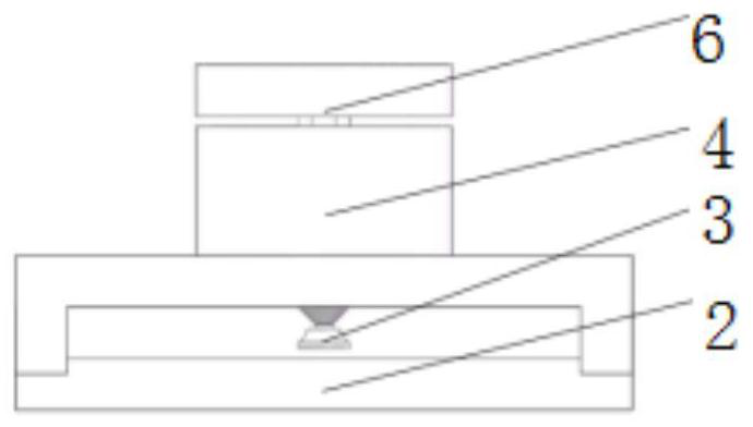
[0035] The embodiment of the present invention discloses a thermocompression sintering fixture for chip packaging, such as figure 1 and 2 As shown, it includes: frame 1, lower heating plate 2, pressure head 3, upper matching cover plate 4, pressure sensor 5, pressure transmission guide rod 6, upper electromagnet 7, lower electromagnet 8, thrust bearing 9, screw rod 10, screw nut 11 and rotating handle 12.

[0036] Wherein, the lower heating plate 2 is instal...


PUM


Abstract

The invention discloses a hot pressing sintering clamp for chip packaging and a chip packaging method. The hot pressing sintering clamp comprises a rack, a lower heating plate, a pressing head, an upper matching cover plate, a pressure sensor, a pressure transmission guide rod, a pressurizing mechanism, a thrust bearing, a lead screw, a lead screw nut and a rotating handle, and the lower heating plate and the upper matching cover plate are precisely matched at the four corners; the parallelism between the upper plate and the lower plate is ensured; and the pressure is controlled by the current in the two mutually exclusive electromagnets. And a spherical hinge structure is arranged between the pressure head and the pressure transmission guide rod, so that the upper surface of the chip can be uniformly pressed when the upper surface of the chip is not parallel to the lower surface of the substrate. The pressure transmission guide rod is precisely matched with the vertical through hole of the upper matching cover plate, so that the perpendicularity between the pressure transmission guide rod and the upper surface of the lower heating plate during pressurization is ensured, and the uniformity of the thickness of the welding flux of the sintering layer can be ensured in the pressurization process; in the heating process, the current of the electromagnet is controlled through pressure feedback, and pressure constant control is achieved.

Description

technical field [0001] The invention relates to the technical field of semiconductor device packaging, and more specifically relates to a packaging fixture and a chip packaging method for hot-pressing sintering of a chip and a base. Background technique [0002] With the rapid development of electronic products and the semiconductor industry, traditional electronic packaging materials can no longer meet the requirements of device heat transfer and service temperature. Nano-solder represented by nano-metal particles has become a current research hotspot, and nano-silver material is considered to be an ideal substitute for traditional solder due to its superior performance. [0003] Compared with the packaging process of traditional solder, nano-solder does not need to be melted during connection, but needs to be sintered under simultaneous heating and pressure conditions. The solder melts during the traditional solder packaging without pressure, so it cannot meet the hot-pre...

Claims


Application Information

Patent Timeline
Patent Type & Authority Applications(China)
IPC IPC(8): H01L21/687H01L21/67H01L21/603
CPCH01L21/67144H01L21/68785H01L21/67253H01L21/67248H01L24/81H01L24/83H01L24/85H01L2224/85203H01L2224/83203H01L2224/81203Y02P70/50
Inventor 吴永超彭鹏郭伟
Owner BEIHANG UNIV
Why Eureka
Try Eureka