
Polarization phase modulator based on two-dimensional germanium selenide and design method of modulator

A phase modulation and design method technology, applied in the direction of polarization components, instruments, optical components, etc., can solve the problems of miniaturization of unfavorable polarization phase modulation devices, achieve efficient and fast identification and detection, simple and clear derivation process, accurate and efficient measurement Effect

Active Publication Date: 2021-05-07
HUAZHONG UNIV OF SCI & TECH +1
View PDF7 Cites 1 Cited by
  • Summary
  • Abstract
  • Description
  • Claims
  • Application Information

AI Technical Summary

Problems solved by technology

According to formula (1), when the wavelength of the incident light remains constant, for the same type of polarization phase modulation device, the lower birefringence effect often leads to a thicker polarization phase modulation device thickness, which is not conducive to the polarization phase modulation device Miniaturization

Method used


Image

  • Polarization phase modulator based on two-dimensional germanium selenide and design method of modulator
  • Polarization phase modulator based on two-dimensional germanium selenide and design method of modulator
  • Polarization phase modulator based on two-dimensional germanium selenide and design method of modulator

Examples


Embodiment Construction

[0066] In order to make the object, technical solution and advantages of the present invention clearer, the present invention will be further described in detail below in conjunction with the accompanying drawings and embodiments. It should be understood that the specific embodiments described here are only used to explain the present invention, not to limit the present invention.

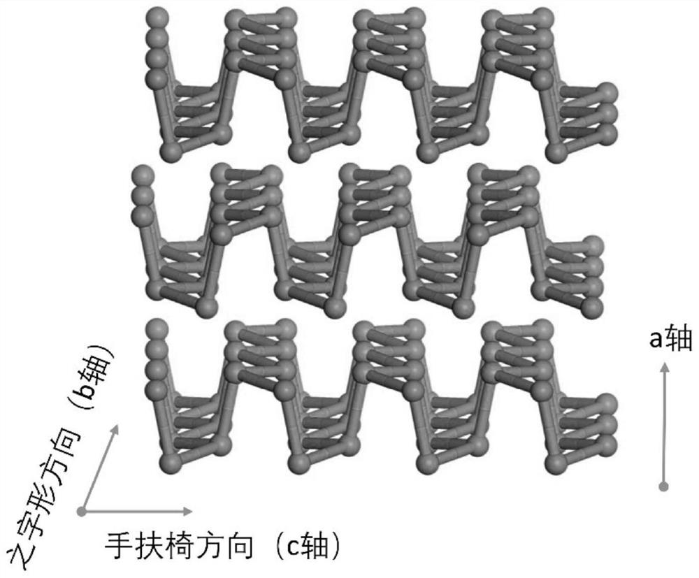
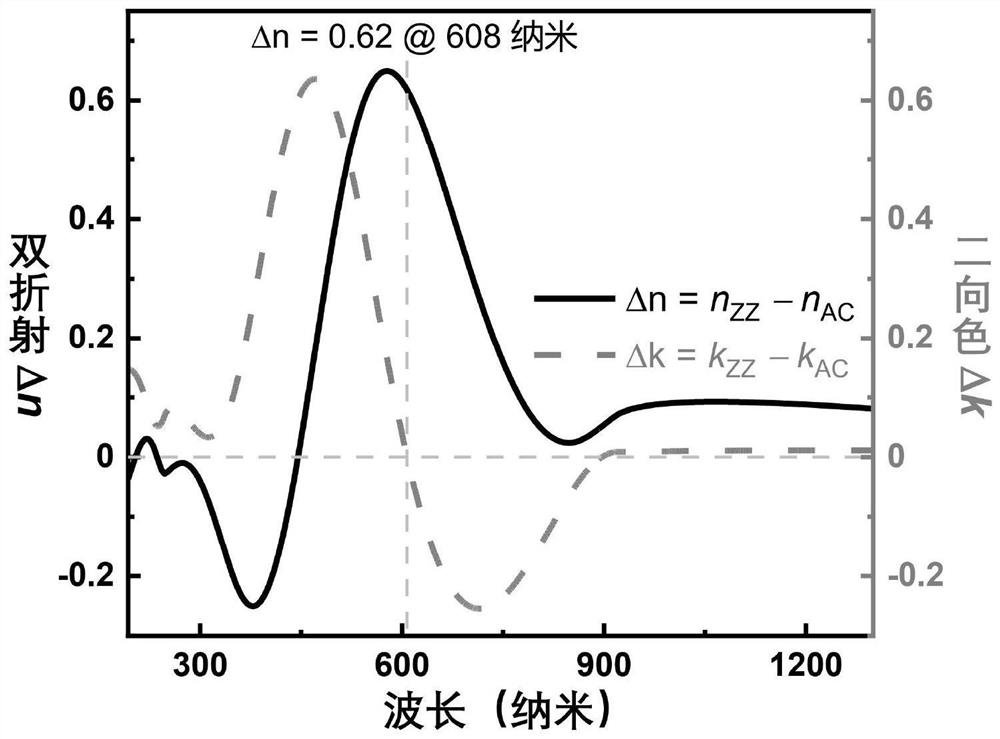
[0067] Since the thickness is often only at the nanometer level or even thinner, the birefringence of two-dimensional materials is mainly caused by the difference in refractive index along the two crystal axes in the plane. It was found that 2D materials with crystal structures with low symmetry tend to have high in-plane birefringence. GeSe is a typical biaxial crystal material (space group is ), the symmetry is lower than that of traditional wave plate materials with uniaxial crystals, theoretical calculations show (Adv. Material. The invention utilizes the high birefringence effect Δn in the...


PUM

PropertyMeasurementUnit
Thicknessaaaaaaaaaa

Abstract

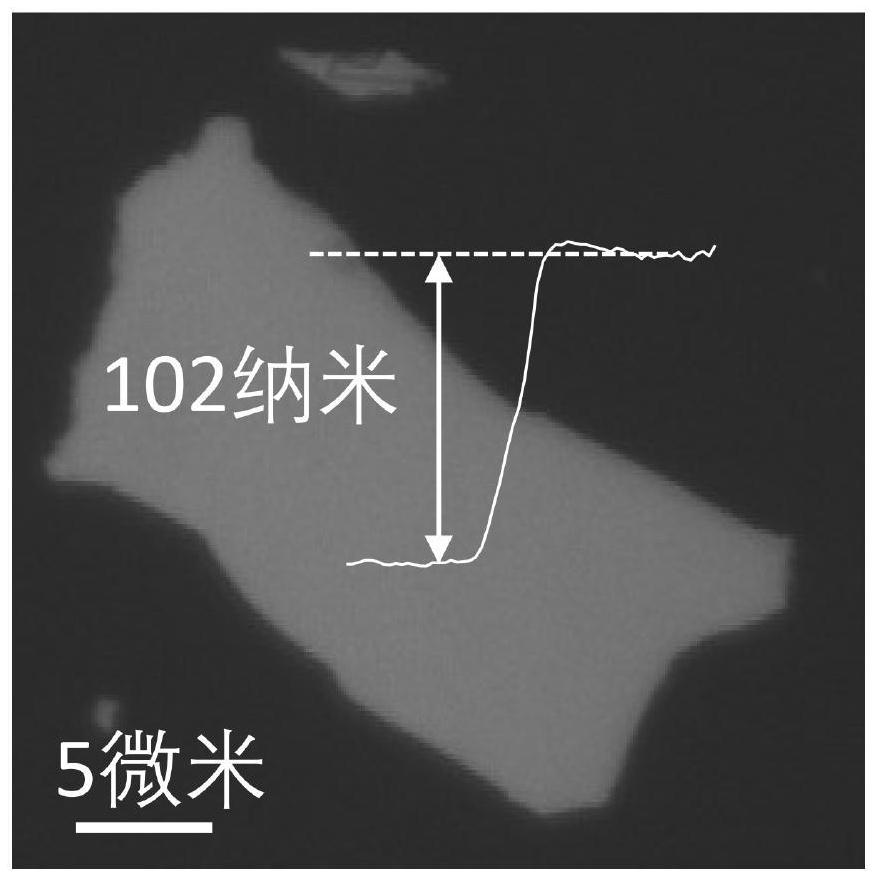
The invention belongs to the field of novel polarization optical devices, and particularly relates to a polarization phase modulator based on two-dimensional germanium selenide and a design method of the modulator. The design method comprises the following steps of: firstly, manufacturing a plurality of two-dimensional GeSe with different thicknesses, attaching the two-dimensional GeSe to a substrate, acquiring in-plane optical constants of the two-dimensional GeSe, calculating phase retardations corresponding to different thicknesses by combining a phase retardation calculation formula, calculating the phase retardations according to the requirements of a target polarization phase modulator on the phase retardations, determining the thickness of the two-dimensional GeSe in the target polarization phase modulator, and finally checking whether the manufactured polarization phase modulator meets the requirement or not through comparison of experimental measurement and calculation fitting. According to the method, the thickness nanocrystallization of the polarization phase modulator can be realized only through simple design, and the method has a very good application prospect.

Description

technical field [0001] The invention belongs to the field of novel polarization optical devices, and more specifically relates to a two-dimensional germanium selenide (GeSe)-based polarization phase modulation device and a design method thereof. Background technique [0002] Traditional optical instruments (such as ellipsometers, etc.) are limited by the size of the instrument, and cannot meet the requirements of in-situ detection of living life and in-situ in-depth detection of large precision instruments, which require small size and have the same or even better functional requirements. Although polarization phase modulation devices made of metasurfaces and metamaterials can also achieve large birefringence effects, their high preparation costs and optical losses make it still a long way to go in practical applications (Nature Photonics, 2018, 12(7): 392 .). [0003] Nano-optical instruments constructed of two-dimensional materials not only have the advantages of small si...

Claims


Application Information

Patent Timeline
IPC IPC(8): G02B1/08G02B5/30G02B27/00G01M11/02
CPCG02B1/08G02B5/3083G02B27/0012G01M11/02
Inventor 魏钟鸣谷洪刚郭正峰刘世元
Owner HUAZHONG UNIV OF SCI & TECH
Learn More