Semiconductor packaging structure and manufacturing method thereof

A packaging structure and manufacturing method technology, which is applied in semiconductor/solid-state device manufacturing, semiconductor devices, semiconductor/solid-state device components, etc., can solve the problems of large chip line loss and thick packaging structure size, etc.

Pending Publication Date: 2021-05-04
NAT CENT FOR ADVANCED PACKAGING +1
View PDF0 Cites 0 Cited by
  • Summary
  • Abstract
  • Description
  • Claims
  • Application Information

AI Technical Summary

Problems solved by technology

[0003] Based on the above problems, the present invention provides a semiconductor packaging structure and its manufacturing method to solve the problem that the size of the semiconductor packaging structure of the front butt-connected chip is relatively thick, and the line loss of the butt-connected chip is relatively large

Method used


Image

  • Semiconductor packaging structure and manufacturing method thereof
  • Semiconductor packaging structure and manufacturing method thereof
  • Semiconductor packaging structure and manufacturing method thereof

Examples


Embodiment 1

[0034]SeeFigure 1 - Figure 10 This embodiment provides a semiconductor package structure, including:

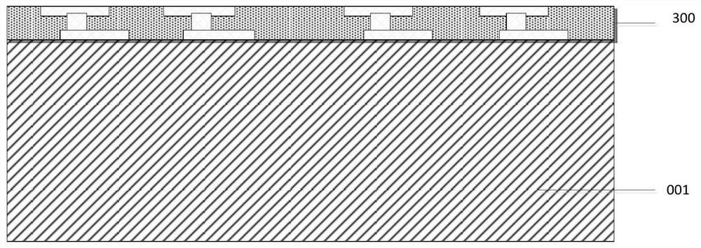
[0035]The first interconnected structure layer 300.

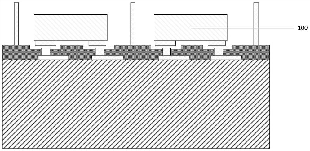
[0036]The first chip layer, the first chip layer is located on the side surface of the first interconnected structure layer 300, and the first chip layer includes a plurality of first chip 100, and the first chip 100 in the first chip layer is facing the first interconnected structure layer. 300 and electrically connected to the first interconnected structure layer 300;

[0037]The second chip layer, the second chip layer is located on one side surface of the first interconnected structure layer 300, and the second chip layer includes a plurality of second chip 200, the second chip layer in the second chip layer is positive. The first interconnected structure layer 300 is electrically connected to the first interconnected structure layer 300.

[0038]The semiconductor package structure of the present embodiment can achieve the first chip 10...

Embodiment 2

[0051]referenceFigure 11 In this embodiment, another semiconductor package structure is provided. The difference from the above-described Embodiment 1 is:

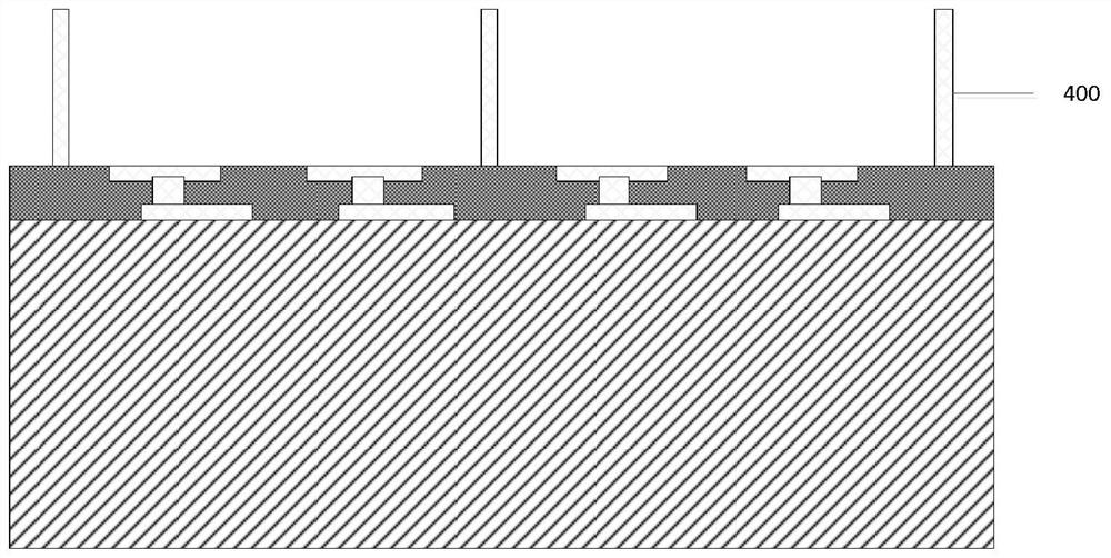
[0052]The second chip layer further includes: a plurality of conductive columns 400 'through the second insulating dielectric layer 210, each of which is electrically connected to the first interconnected structure layer 300, and the surface of the other end and the second insulating dielectric layer. 210 is parallel from the surface of the first interconnected layer 300.

[0053]The semiconductor package structure also includes a second interconnected layer 500 ', and the second interconnected structure layer 500' is located from the surface of the second chip layer away from the surface of the first interconnected structure layer 300, the second interconnected structure layer 500 'and a plurality of conductive columns 400 'Electrical connection;

[0054]The semiconductor package structure of the present embodiment, the second insulatin...

Embodiment 3

[0057]referenceFigure 1 - Figure 10 This embodiment provides a method of manufacturing a semiconductor package structure, including the following steps:

[0058]The first interconnected structure layer 300 is formed.

[0059]The first chip layer is formed, and the first chip layer is formed on one side surface of the first interconnected structure layer 300, and the first chip layer includes a plurality of first chip 100, and the first chip layer in the first chip layer is facing the first interconnection. The structural layer 300 is electrically connected to the first interconnected structure layer 300.

[0060]The second chip layer is formed, and the second chip layer is formed on one side surface of the first interconnected layer 300 to the first chip layer, and the second chip layer includes a plurality of second chip 200, the second chip 200 in the second chip layer 200. The front is electrically connected to the first interconnected structure layer 300 and is electrically connected to ...


PUM


Abstract

The invention provides a semiconductor packaging structure, which comprises a first interconnection structure layer, a first chip layer and a second chip layer, wherein the first chip layer is located on the surface of one side of the first interconnection structure layer, the first chip layer comprises a plurality of first chips, and the front surfaces of the first chips in the first chip layer face the first interconnection structure layer and are electrically connected with the first interconnection structure layer; the second chip layer is located on the surface of the side, back to the first chip layer, of the first interconnection structure layer, the second chip layer comprises a plurality of second chips, and the front surfaces of the second chips in the second chip layer face the first interconnection structure layer and are electrically connected with the first interconnection structure layer; and the front faces of the second chips in the first chip layer and the second chip layer face the first interconnection structure layer, and opposite welding is achieved through the first interconnection structure layer. The opposite surfaces of the chips needing to be butted are directly welded, line transmission loss can be effectively reduced, compared with solder ball welding, the thickness of the first interconnection structure layer between the chips is relatively thin, and the overall thickness of the packaging structure can be effectively reduced.

Description

Technical field[0001]The present invention relates to the field of semiconductor chip interconnection, and more particularly to a semiconductor package structure and a method of manufacturing the same.Background technique[0002]In the semiconductor package structure, the front side of the relative chip is usually docked with tin balls. Silk ball docking package structure, solder ball due to the process, usually itself is large, and thus the portion between the docked chips is thick, affecting the thinning of the unit of the package structure. And because the tin ball is large, the line between the docked chips is long, and the line loss is also large.Inventive content[0003]Based on the above problem The present invention provides a semiconductor package structure and a manufacturing method thereof to solve the size of the semiconductor package structure of the front-docked chip, and a large problem of line loss of the docking chip.[0004]The present invention provides a semiconductor ...

Claims


Application Information

Patent Timeline
Patent Type & Authority Applications(China)
IPC IPC(8): H01L25/065H01L21/98H01L23/488H01L23/538H01L23/31H01L21/50H01L21/56
CPCH01L21/50H01L21/56H01L23/3185H01L23/488H01L23/538H01L24/83H01L25/0652H01L25/50H01L2224/83801
Inventor 王国军曹立强严阳阳
Owner NAT CENT FOR ADVANCED PACKAGING
Why Eureka
Try Eureka