
Semiconductive shielding material and preparation method and application thereof

A technology of semi-conductive and shielding materials, which is applied to power cables, conductors, and circuits with shielding layers/conductive layers, and can solve problems such as cracking of the outer screen, separation of the insulating layer from the shielding layer, and insufficient purity of nitrogen gas in vulcanized tubes. The preparation steps are simple, easy to obtain, and suitable for mass production

Active Publication Date: 2021-04-30
ZHEJIANG WANMA MACROMOLECULE MATERIAL
View PDF6 Cites 4 Cited by
  • Summary
  • Abstract
  • Description
  • Claims
  • Application Information

AI Technical Summary

Problems solved by technology

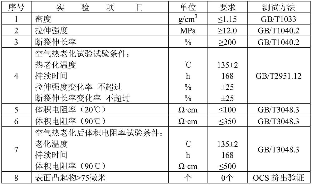
[0005] In view of the technical problems in the existing technology, the nitrogen purity of the vulcanized tube in the cable factory is not enough, resulting in the occasional cracking of the outer screen when producing 110kV large square cables; Layer separation and other phenomena; the invention firstly provides a semi-conductive shielding material, which can solve the separation between the insulating layer and the shielding layer, and can also prevent stress cracking of large square high-voltage cables during production

Method used


Image

  • Semiconductive shielding material and preparation method and application thereof
  • Semiconductive shielding material and preparation method and application thereof
  • Semiconductive shielding material and preparation method and application thereof

Examples


preparation example Construction

[0049] The present invention also provides a method for preparing the semiconductive shielding material according to the present invention, which includes the step of mixing the components of the semiconductive shielding material.

[0050] Specifically, the preparation method comprises the following steps:

[0051] Premixing PE wax, dispersant, antioxidant and zinc stearate to obtain a premix;

[0052] Take ethylene-butyl acrylate copolymer, high-density polyethylene and conductive carbon black for initial mixing, then add the premix and mix again to obtain cooked glue;

[0053] The cooked rubber is extruded and granulated to obtain a semi-conductive shielding material.

[0054] Further, the preparation method may include the following steps:

[0055] (1) Add PE wax, dispersant, antioxidant and zinc stearate to the blender for premixing to obtain a premix;

[0056] (2) Add ethylene-butyl acrylate copolymer, high-density polyethylene and conductive carbon black to the intern...

Embodiment 1

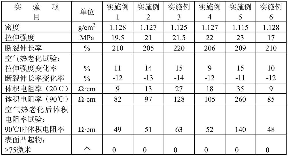
[0069] Step 1: Take 1.2 parts of PE wax with a number average molecular weight of 3000-5000, 0.3 parts of multifunctional dispersant TEGOdispersers 760W, and 0.4 parts of antioxidant 4,4'-thiobis(6-tert-butyl-m-cresol) , 2.1 parts of zinc stearate, added into a blender for premixing to obtain a premix.

[0070] Step 2: Take 50 parts of ethylene-butyl acrylate copolymer, 6 parts of high-density polyethylene, and 40 parts of Cabot carbon black VXC50040, put them into the internal mixer for the first closed mixing for 60 seconds, and then add the pretreated one in step 1 The premix is ​​closed and mixed again for 300 seconds, and the mature rubber is mixed. During the process, the cooling water needs to be turned on to ensure that the temperature of the material is lower than 180°C;

[0071] Step 3: Send the mixed cooked rubber into the twin-screw for extrusion and strand granulation, pass the obtained particles through a vibrating sieve to screen out irregular particles, absorb ...

Embodiment 2

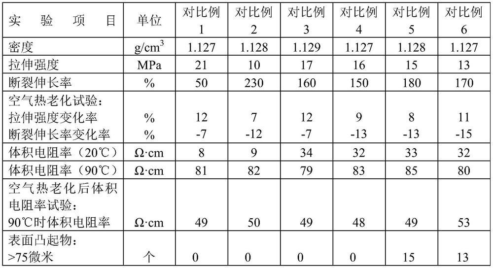
[0073] The difference between this example and Example 1 is that 49.5 parts of ethylene-butyl acrylate copolymer, 6 parts of high-density polyethylene, 39.5 parts of Cabot carbon black VXC500, and the rest of the composition are the same as in Example 1. And the preparation process of Example 2 is the same as that of Example 1, and the semi-conductive shielding material is prepared.


PUM

PropertyMeasurementUnit
melt flow indexaaaaaaaaaa
tensile strengthaaaaaaaaaa

Abstract

The invention provides a semiconductive shielding material and a preparation method and application thereof. The semiconductive shielding material comprises the following components: an ethylene-butyl acrylate copolymer, high-density polyethylene, conductive carbon black, PE wax, zinc stearate, a dispersing agent and an antioxidant. The mass ratio of the ethylene-butyl acrylate copolymer to the high-density polyethylene is 1:(0.05-0.2), preferably 1:(0.07-0.1). According to the semiconductive shielding material, the ethylene-butyl acrylate copolymer is used as a matrix, and the high-density polyethylene is added, so that the material has a skeleton supporting effect after being extruded, an insulating layer is prevented from being separated from a shielding layer, and a stress cracking phenomenon in a vulcanization process is prevented.

Description

technical field [0001] The invention relates to a semiconductive shielding material and its preparation method and application, in particular to a low thermal shrinkage ultra-smooth semiconductive shielding material for a 110kV large square cable and a preparation method thereof, belonging to the technical field of high-voltage cable material production. Background technique [0002] A cable usually consists of a conductor, an inner shield, an insulation layer, an outer shield and a sheath. ICE stipulates that cables with a voltage level of 6kV and above should have an inner shielding layer and an outer shielding layer. The conductor is twisted by multiple wires, and its surface is not smooth, and it is easy to form a gap with the insulating layer to cause the electric field to concentrate. An inner shielding layer of semi-conductive material is set on the surface of the conductor, which is at the same potential as the shielded conductor. And achieve good contact with the i...

Claims


Application Information

Patent Timeline
Patent Type & Authority Applications(China)
IPC IPC(8): C08L23/08C08L23/06C08K3/04C08K5/098H01B7/17H01B9/02
CPCC08L23/0869H01B7/17H01B9/02C08L2203/202C08L2207/062C08L2205/025C08L2205/03C08K2201/001C08L23/06C08K3/04C08K5/098Y02A30/14
Inventor 俞杰陈胜立杨强李秀娟堵志祥陈卓赵淑群
Owner ZHEJIANG WANMA MACROMOLECULE MATERIAL
Learn More