
Patsnap Eureka
For R&D, Patsnap Eureka makes reading and utilizing patents & technical documents easy.
Patsnap Eureka AIR
Designed for self-driven R&D workflows. Generate viable solutions, solve complex R&D challenges, empower your innovation with AI.

Patsnap Eureka Materials
Designed for material experts only. Revolutionize your material R&D, from search, analyze, to developing new materials.

TechResearch
Generate reliable direction feasibility study reports for your R&D in just a few steps.

TechSeek
Discover and master advanced knowledge NOW. Basics, ideas, possibilities, all at once.

TechMind
As an expert in R&D Theories, TechMind can generates customized viable solutions instantly.

TechRisk
Analyze your overall solution with one click, know your potential R&D risks in advance.

TechMonitor
Get weekly tech updates, stay abreast of the latest tech innovations and key insights.
Preparation method of gas sensor and gas sensor
A gas sensor and N-type semiconductor technology, applied in the direction of semiconductor devices, electrical components, material resistance, etc., can solve the problems of increasing device on-resistance and operating voltage, reducing device performance, and deteriorating the quality of nanowire crystals, etc., to achieve low Effect of operating voltage and low contact resistance
- Summary
- Abstract
- Description
- Claims
- Application Information
AI Technical Summary
Problems solved by technology
Method used
Image


Examples
Embodiment Construction
[0013] A method for preparing a gas sensor provided by the present invention and specific implementations of the gas sensor will be described in detail below with reference to the accompanying drawings.
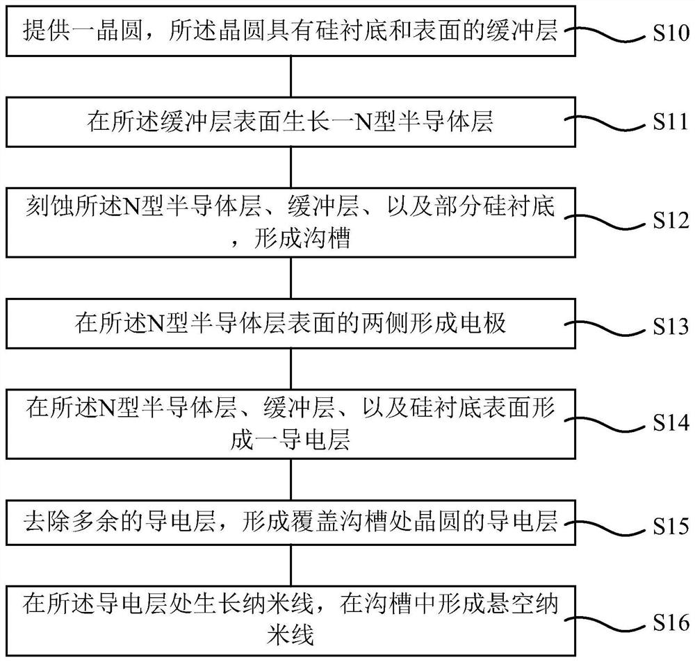
[0014] attached figure 1 Shown is a schematic diagram of the steps of a specific embodiment of the present invention, including: step S10, providing a wafer, the wafer has a silicon substrate and a buffer layer on the surface; step S11, growing a N on the surface of the buffer layer type semiconductor layer; step S12, etching the N-type semiconductor layer, buffer layer, and part of the silicon substrate to form a trench; step S13, forming electrodes on both sides of the surface of the N-type semiconductor layer; step S14, The N-type semiconductor layer, the buffer layer, and the surface of the silicon substrate form a conductive layer; step S15, remove the redundant conductive layer, and form a conductive layer covering the wafer at the trench; step S16, grow on the conducti...
PUM
| Property | Measurement | Unit |
|---|---|---|
| thickness | aaaaa | aaaaa |
| thickness | aaaaa | aaaaa |
| thickness | aaaaa | aaaaa |
Abstract
Description
Claims
Application Information
 - R&D Engineer
- R&D Manager
- IP Professional
- Industry Leading Data Capabilities
- Powerful AI technology
- Patent DNA Extraction
Browse by: Latest US Patents, China's latest patents, Technical Efficacy Thesaurus, Application Domain, Technology Topic, Popular Technical Reports.
© 2024 PatSnap. All rights reserved.Legal|Privacy policy|Modern Slavery Act Transparency Statement|Sitemap|About US| Contact US: help@patsnap.com