
A semiconductor crystal growth device

A crystal growth and semiconductor technology, applied in the directions of crystal growth, single crystal growth, single crystal growth, etc., can solve problems such as control of unfavorable crystal growth quality, and achieve the goal of improving crystal pulling quality, reducing defects, and improving speed uniformity. Effect

Active Publication Date: 2022-02-01
ZING SEMICON CORP
View PDF0 Cites 0 Cited by
  • Summary
  • Abstract
  • Description
  • Claims
  • Application Information

AI Technical Summary

Problems solved by technology

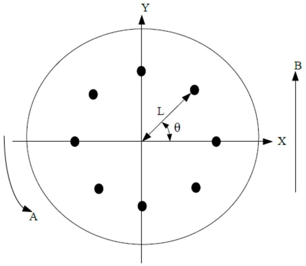
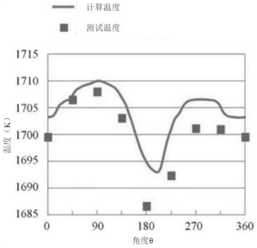
Because, in the semiconductor crystal growth process, the temperature below the interface between the semiconductor crystal and the melt presents periodic fluctuations with the change of the circumference angle, that is, the Gc of the temperature gradient (dT / dZ) of the crystal and the melt as the interface, Gm fluctuates, therefore, the crystallization speed PS of the crystal in the circumferential angle direction fluctuates periodically, which is not conducive to the control of crystal growth quality

Method used


Image

  • A semiconductor crystal growth device
  • A semiconductor crystal growth device
  • A semiconductor crystal growth device

Examples


Embodiment Construction

[0036] In the following description, numerous specific details are given in order to provide a more thorough understanding of the present invention. It will be apparent, however, to one skilled in the art that the present invention may be practiced without one or more of these details. In other examples, some technical features known in the art are not described in order to avoid confusion with the present invention.

[0037] For a thorough understanding of the present invention, a detailed description will be set forth in the following description to illustrate the semiconductor crystal growth apparatus of the present invention. Obviously, the practice of the invention is not limited to specific details familiar to those skilled in the semiconductor arts. Preferred embodiments of the present invention are described in detail below, however, the present invention may have other embodiments besides these detailed descriptions.

[0038] It should be noted that the terms used h...


PUM

PropertyMeasurementUnit
angleaaaaaaaaaa
radiusaaaaaaaaaa

Abstract

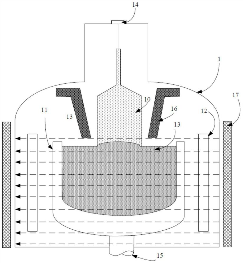
The invention provides a semiconductor crystal growth device. It includes: a furnace body; a crucible, which is arranged inside the furnace body, to accommodate silicon melt; a lifting device, which is arranged on the top of the furnace body, to extract silicon melt from the silicon melt Pull out the silicon crystal rod; the guide tube, the guide tube is barrel-shaped and arranged vertically above the silicon melt in the furnace body; the pulling device pulls the silicon The crystal rod passes through the guide tube in the vertical direction; and the magnetic field applying device is used to apply a horizontal magnetic field to the silicon melt in the crucible; wherein, the bottom of the guide tube is provided with There is a downward protruding step, so that the distance between the bottom of the draft tube and the silicon melt surface in the direction of the magnetic field is smaller than the distance between the silicon melt surface and the direction perpendicular to the magnetic field. distance between body fluid surfaces. According to the semiconductor crystal growth apparatus of the present invention, the quality of semiconductor crystal growth is improved.

Description

technical field [0001] The invention relates to the field of semiconductor manufacturing, in particular to a semiconductor crystal growth device. Background technique [0002] The Czochralski method (Cz) is an important method for preparing silicon single crystals for semiconductors and solar energy. The high-purity silicon material placed in the crucible is heated to melt it through a thermal field composed of carbon materials, and then the seed crystal is immersed in the In the melt and through a series of processes (seeding, shouldering, equal diameter, finishing, cooling), a single crystal rod is finally obtained. [0003] In the crystal growth of semiconductor single crystal silicon or solar single crystal silicon using the CZ method, the temperature distribution of the crystal and the melt directly affects the quality and growth rate of the crystal. During the growth of CZ crystal, due to the existence of thermal convection in the melt, the distribution of trace impur...

Claims


Application Information

Patent Timeline
Patent Type & Authority Patents(China)
IPC IPC(8): C30B30/04C30B15/00C30B29/06
CPCC30B15/14C30B29/06C30B15/305C30B15/20C30B15/22C30B30/04
Inventor 沈伟民王刚邓先亮黄瀚艺赵言
Owner ZING SEMICON CORP
Learn More