Semiconductor structure and forming method thereof

A technology of semiconductors and conductive layers, which is applied in the manufacture/processing of components of electromagnetic equipment, resistors controlled by magnetic fields, and electromagnetic devices, and can solve problems such as poor performance of magnetic random access memory

Active Publication Date: 2021-04-09
SEMICON MFG INT (SHANGHAI) CORP +1
View PDF14 Cites 1 Cited by
  • Summary
  • Abstract
  • Description
  • Claims
  • Application Information

AI Technical Summary

Problems solved by technology

[0004]However, prior art MRAMs have poor performance

Method used


Image

  • Semiconductor structure and forming method thereof
  • Semiconductor structure and forming method thereof
  • Semiconductor structure and forming method thereof

Examples


Embodiment Construction

[0031] As mentioned in the background, currently formed semiconductor structures perform poorly.

[0032] The reasons for the poor performance of the semiconductor structure will be described in detail below in conjunction with the accompanying drawings. Figure 1 to Figure 6 It is a structural schematic diagram of each step of a method for forming a semiconductor structure.

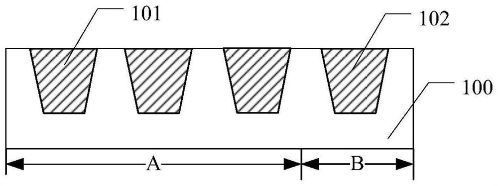
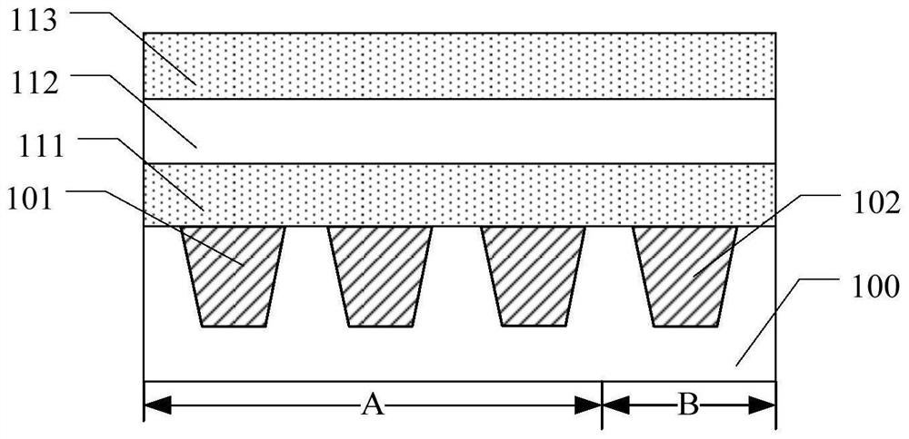
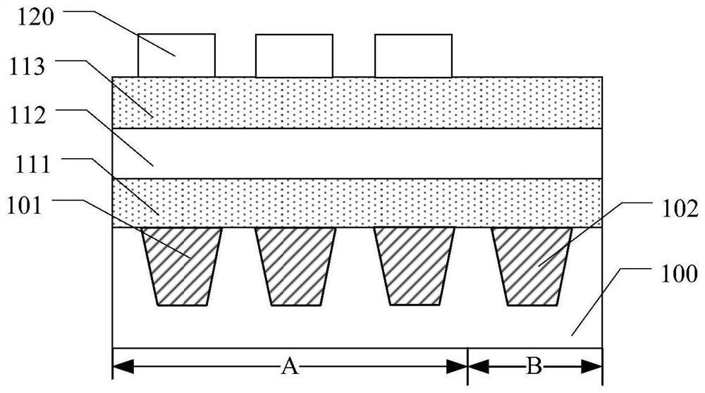
[0033] Please refer to figure 1 , providing a substrate 100, the substrate 100 includes a storage area A and a logic area B, the storage area A has a first conductive layer 101, the logic area B has a second conductive layer 102, and the substrate 100 is exposed The top surface of the first conductive layer 101 and the top surface of the second conductive layer 102 are shown.

[0034] Please refer to figure 2 , forming a first electrode film 111 , a magnetic tunnel film 112 on the surface of the first electrode film 111 , and a second electrode film 113 on the surface of the magnetic tunnel film 112 ...


PUM


Abstract

The invention relates to a semiconductor structure and a forming method thereof, and the method comprises the steps: providing a substrate which is internally provided with a first conductive layer extending in a first direction and being arranged in a second direction, forming initial magnetic tunnel structures on the surface of the first conductive layer and the surface of the substrate; forming a first trench and a second trench in the initial magnetic tunnel structure, the second trench extending in a first direction, the first trench being located between adjacent second trenches, the first trench extending in a second direction, the first trench having a first size in the first direction, the second trench having a second size in the second direction, the first size being smaller than the second size; forming mask layers in the first trench and on the surfaces of the side walls of the second trench, the first trench is filled with the mask layers; and etching the initial magnetic tunnel structures by taking the mask layers as masks until the surface of the substrate is exposed, and forming a magnetic tunnel structure on the surface of the first conductive layer. The semiconductor structure formed by the method is good in performance.

Description

technical field [0001] The invention relates to the technical field of semiconductor manufacturing, in particular to a semiconductor structure and a forming method thereof. Background technique [0002] MRAM (Magnetic Random Access Memory) is a non-volatile magnetic random access memory. It has the high-speed read and write capabilities of static random access memory (SRAM), high integration of dynamic random access memory (DRAM) and power consumption far lower than DRAM, compared with flash memory (Flash), with the use of time Increase performance without degradation. Due to the above-mentioned characteristics of MRAM, it is called universal memory and is considered to be able to replace SRAM, DRAM, EEPROM and Flash. [0003] Unlike traditional random access memory chip fabrication technology, data in MRAM is not stored in the form of charge or current, but in a magnetic state, and is sensed by measuring resistance without disturbing the magnetic state. MRAM uses a magne...

Claims


Application Information

Patent Timeline
Patent Type & Authority Applications(China)
IPC IPC(8): H01L43/12H01L43/08H01L43/02
CPCH10N50/80H10N50/10H10N50/01
Inventor 金吉松
Owner SEMICON MFG INT (SHANGHAI) CORP
Why Eureka
Try Eureka