Method and device for optimizing current distribution, integrated circuit chip and electronic equipment

A technology of current distribution and chips, which is applied in the direction of circuits, electrical components, electric solid devices, etc., can solve problems such as unbalanced current distribution

Active Publication Date: 2021-04-02
HYGON INFORMATION TECH CO LTD
View PDF5 Cites 1 Cited by
  • Summary
  • Abstract
  • Description
  • Claims
  • Application Information

AI Technical Summary

Problems solved by technology

[0006] In view of this, the purpose of this application is to provide a method, device, integrated circuit chip and electronic equipment for optimizing current distribution, so as to improve the problem of unbalanced distribution of current on the via hole VIA

Method used


Image

  • Method and device for optimizing current distribution, integrated circuit chip and electronic equipment
  • Method and device for optimizing current distribution, integrated circuit chip and electronic equipment
  • Method and device for optimizing current distribution, integrated circuit chip and electronic equipment

Examples


Embodiment approach

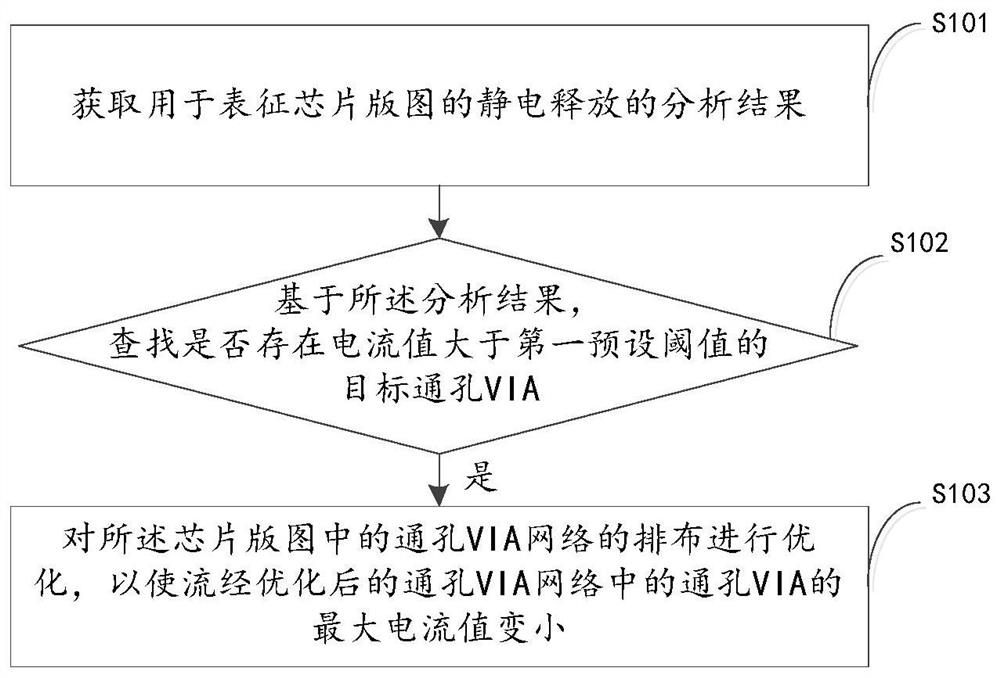
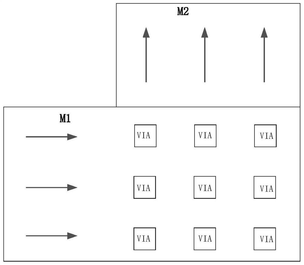
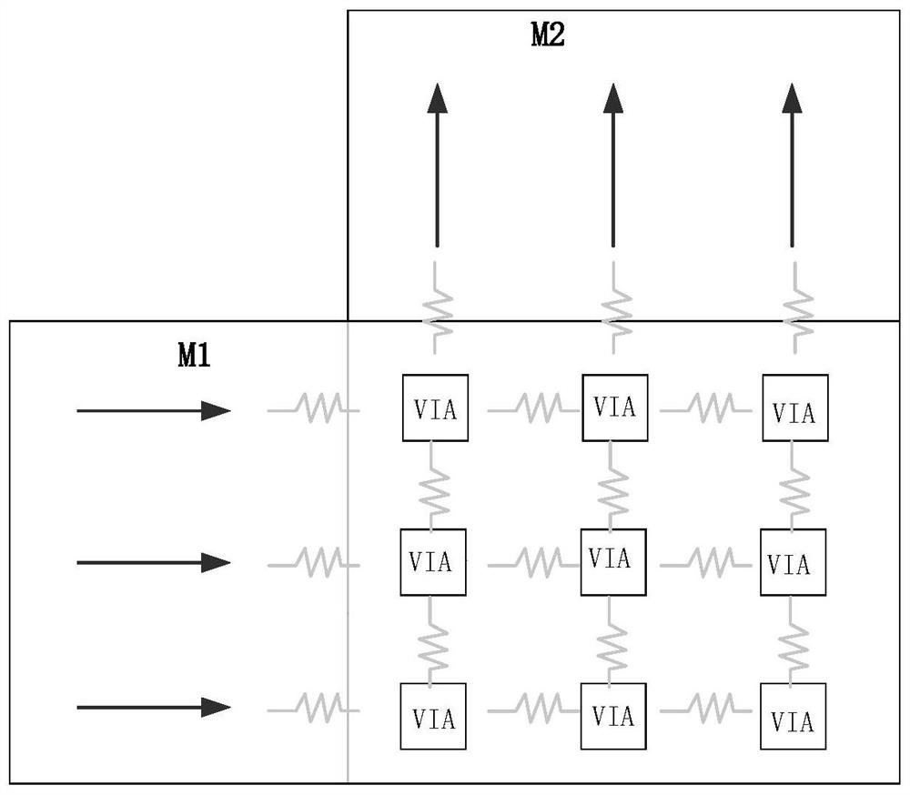
[0043] Wherein, in one embodiment, when optimizing the arrangement of the via VIA network in the chip layout, it may be optimized only the arrangement of the via VIA network on the path where the target via VIA is located. In this implementation manner, the arrangement of the via VIA network on the paths where the other via VIAs except the target via VIA are located may not be optimized. Since the through-hole VIA network on the path where the target through-hole VIA is located shares a large amount of current, by optimizing it, the maximum current value flowing through the through-hole VIA in the optimized through-hole VIA network becomes smaller.

[0044] In addition, in addition to finding whether there is a target via VIA whose current value is greater than the first preset threshold based on the analysis result, it is also possible to find whether there is a target via VIA whose current value is smaller than the second preset threshold based on the analysis result, Wherei...


PUM


Abstract

The invention relates to a method and device for optimizing current distribution, an integrated circuit chip and electronic equipment, and belongs to the technical field of integrated circuits. The method comprises the steps of obtaining an analysis result used for representing electrostatic discharge of a chip layout; searching whether a target through hole VIA of which the current value is greater than a first preset threshold exists or not based on the analysis result; and when the target through hole VIA of which the current value is greater than the first preset threshold exists, optimizing the arrangement of the through hole VIA network in the chip layout, so that the maximum current value flowing through the through hole VIA in the optimized through hole VIA network is reduced. On the basis of an analysis result representing electrostatic discharge of the chip layout, when a target through hole VIA of which the current value is greater than a first preset threshold is found, thearrangement of a through hole VIA network in the chip layout is optimized, so that the maximum current value flowing through the through hole VIA in the optimized through hole VIA network is reduced,and the problem of unbalanced distribution of current on the through hole VIA is solved.

Description

technical field [0001] The application belongs to the technical field of integrated circuits, and in particular relates to a method and device for optimizing current distribution, an integrated circuit chip and electronic equipment. Background technique [0002] With the continuous improvement of semiconductor manufacturing process, the gate length of Field-Effect Transistor (FET) has changed from 90nm, 40nm, and 28nm in the past to 16nm and 7nm in the current FinFET (Fin Field-Effect Transistor) process. Under the condition of the same metal line width, as the thickness of the metal layer decreases, the cross-sectional area of ​​the metal line also decreases year-on-year, so the over-current capability of the metal line becomes weaker, but the market has a strong demand for products that are resistant to Electro-Static discharge (ESD) ) current requirements have not changed. For example, the metal connection wires must also meet the Electro Migration (EM) capability require...

Claims


Application Information

Patent Timeline
Patent Type & Authority Applications(China)
IPC IPC(8): H01L27/02H01L23/60H01L23/538
CPCH01L27/0207H01L27/0292H01L23/5384H01L23/60
Inventor 冯东东杨洋
Owner HYGON INFORMATION TECH CO LTD
Why Eureka
Try Eureka