Electronic component and method for manufacturing electronic component

A technology of electronic parts and manufacturing methods, which is applied in the direction of resistor manufacturing, capacitor manufacturing, and electrical component assembly of printed circuits, etc., can solve the problems of complicated positioning operations, difficult positioning, time-consuming, etc., and achieve simplified bonding operations, improved forming speed, The effect of reducing manufacturing costs

Inactive Publication Date: 2021-03-30
MITSUBISHI MATERIALS CORP
View PDF9 Cites 0 Cited by
  • Summary
  • Abstract
  • Description
  • Claims
  • Application Information

AI Technical Summary

Problems solved by technology

[0011] However, the methods described in Patent Documents 3 and 4 are time-consuming and costly
On the other hand, the Au-Sn flakes described in Patent Document 2 are hard and brittle, and it takes time to process them into various shapes of preforms.
In addition, since the Au-Sn flake-shaped preform is thin and small, it is difficult to position it between electronic components and substrates and other bonding objects, and the positioning work is complicated.

Method used


Image

  • Electronic component and method for manufacturing electronic component
  • Electronic component and method for manufacturing electronic component
  • Electronic component and method for manufacturing electronic component

Examples


Embodiment Construction

[0041] Hereinafter, the electronic component and the manufacturing method of the electronic component which concern on this invention are demonstrated using drawing.

[0042] [Schematic structure of electronic parts]

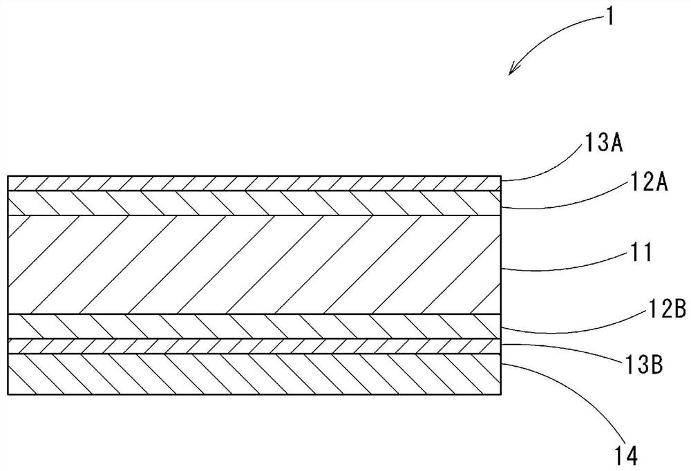
[0043] figure 1 It is a sectional view showing the electronic component 1 of this embodiment.

[0044] Such as figure 1 As shown, an electronic component 1 used as a thermistor or capacitor includes: a ceramic element 11; glass-containing Au layers 12A, 12B formed on both sides of the ceramic element 11; pure Au layers 13A, 13B formed on glass-containing Au layers 12A, 12B; and Au—Sn alloy layer 14, formed on pure Au layer 13B.

[0045] The electronic component 1 is fixed to a bonding object such as a substrate (not shown). Specifically, the electronic component 1 is bonded by disposing the Au—Sn alloy layer 14 of the electronic component 1 on the bonding surface of the bonding object, heating it, and cooling the molten Au—Sn alloy layer 14 to solidify it. ...


PUM


Abstract

The invention provides an electronic component that can be easily bonded to a bonding target and a method for manufacturing the electronic component. The electronic component comprises a ceramic element, glass-containing Au layers formed on both surfaces of the ceramic element, and an Au-Sn alloy layer formed on at least one of the glass-containing Au layers. The electronic component further comprises a pure Au layer between the glass-containing Au layer and the Au-Sn alloy layer. Furthermore, the Au-Sn alloy layer has an Au-Sn eutectic structure.

Description

technical field [0001] The present invention relates to an electronic component such as a thermistor or a capacitor, and a method for manufacturing the electronic component. This application claims priority based on Japanese Patent Application No. 2018-154404 filed on August 21, 2018, and uses the content thereof here. Background technique [0002] Conventionally, electronic components such as a thermistor and a capacitor in which a metal film (metal layer) is formed on both surfaces of a ceramic element are known. For example, in the positive temperature coefficient thermistor device disclosed in Patent Document 1, a moisture-resistant aluminum electrode as the metal layer is formed on the surface of the PTC thermistor element (semiconductor). As a method of forming such a metal layer of an electronic component, a method of applying an aluminum paste containing glass frit and firing it is described (see Patent Document 1). [0003] Such an electronic component is bonded t...

Claims


Application Information

Patent Timeline
IPC IPC(8): H01C7/04H01G13/00H05K3/34H01C1/01H01C7/02H01C17/00H01F27/06H01G2/06
CPCH05K3/34H01C1/01H01C7/04H01C7/02H01F27/06H01G2/06B32B17/061C04B41/90C04B2111/00844C04B41/009C04B41/52H01C7/008H01C7/021H01C17/06513C04B35/01C04B41/4539C04B41/5022C04B41/5116C04B41/4529C04B41/522C04B41/5161H01C17/00H01G13/00B32B18/00B32B2250/40B32B2255/205B32B2307/202B32B2309/02B32B2311/04B32B2311/16B32B2315/02B32B2315/08B32B2457/00
Inventor 石川雅之大道悟西泽薫吉田彰宏佐藤博树
Owner MITSUBISHI MATERIALS CORP
Why Eureka
Try Eureka