Temperable off-line net-color high-transmittance silver-free LOW-E coated glass and preparation method thereof
A coated glass, high-transparency technology, applied in the coating and other directions, can solve the problems of low radiation resistance, inability to lighten the structure, and limited use occasions.
- Summary
- Abstract
- Description
- Claims
- Application Information
AI Technical Summary
Problems solved by technology
Method used
Image
Examples
Embodiment 1
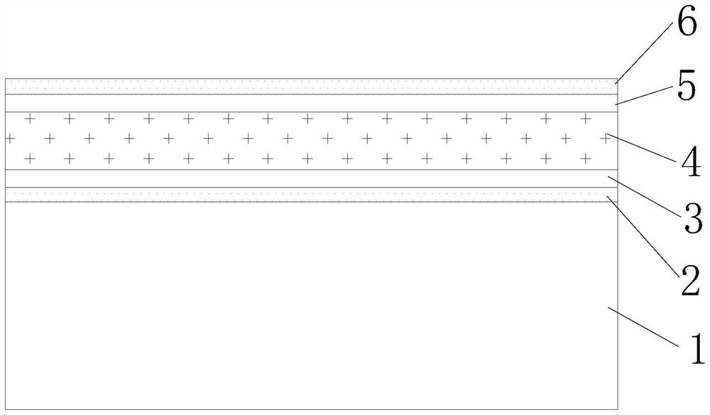
[0021] A kind of toughened off-line pure color high-transparency silver-free LOW-E coated glass, including a glass substrate on which a first dielectric layer, a second dielectric layer, a functional layer, and a third layer are sequentially sputtered from bottom to top A dielectric layer and a fourth dielectric layer, the first dielectric layer and the fourth dielectric layer are silicon nitride layers, the second dielectric layer and the third dielectric layer are silicon oxide layers, and the functional layer is indium tin oxide layer.
[0022] The indium tin oxide layer includes 80% indium oxide, 20% tin oxide and very few impurities by weight; the thickness of the first dielectric layer is 16nm, the thickness of the second dielectric layer is 23nm, and the functional layer The thickness of the dielectric layer is 220nm, the thickness of the third dielectric layer is 27nm, and the thickness of the fourth dielectric layer is 18nm.
[0023] A method for preparing toughened ...
Embodiment 2
[0029] A kind of toughened off-line pure color high-transparency silver-free LOW-E coated glass, including a glass substrate on which a first dielectric layer, a second dielectric layer, a functional layer, and a third layer are sequentially sputtered from bottom to top A dielectric layer and a fourth dielectric layer, the first dielectric layer and the fourth dielectric layer are silicon nitride layers, the second dielectric layer and the third dielectric layer are silicon oxide layers, and the functional layer is indium tin oxide layer.
[0030] The indium tin oxide layer includes 90% indium oxide, 10% tin oxide and very few impurities by weight; the thickness of the first dielectric layer is 22nm, and the thickness of the second dielectric layer is 30nm. The thickness of the layer is 250nm, the thickness of the third dielectric layer is 36nm, and the thickness of the fourth dielectric layer is 25nm.
[0031] A preparation method of toughened off-line pure color high-transp...
Embodiment 3
[0036] A kind of toughened off-line pure color high-transparency silver-free LOW-E coated glass, including a glass substrate on which a first dielectric layer, a second dielectric layer, a functional layer, and a third layer are sequentially sputtered from bottom to top A dielectric layer and a fourth dielectric layer, the first dielectric layer and the fourth dielectric layer are silicon nitride layers, the second dielectric layer and the third dielectric layer are silicon oxide layers, and the functional layer is indium tin oxide layer.
[0037] The indium tin oxide layer includes 85% indium oxide, 15% tin oxide and very few impurities by weight; the thickness of the first dielectric layer is 19nm, and the thickness of the second dielectric layer is 26nm. The thickness of the layer is 235nm, the thickness of the third dielectric layer is 32nm, and the thickness of the fourth dielectric layer is 22nm.
[0038] A preparation method of toughened off-line pure color high-transp...
PUM
| Property | Measurement | Unit |
|---|---|---|
| Thickness | aaaaa | aaaaa |
| Thickness | aaaaa | aaaaa |
| Thickness | aaaaa | aaaaa |
Abstract
Description
Claims
Application Information
 - R&D
- Intellectual Property
- Life Sciences
- Materials
- Tech Scout
- Unparalleled Data Quality
- Higher Quality Content
- 60% Fewer Hallucinations
Browse by: Latest US Patents, China's latest patents, Technical Efficacy Thesaurus, Application Domain, Technology Topic, Popular Technical Reports.
© 2025 PatSnap. All rights reserved.Legal|Privacy policy|Modern Slavery Act Transparency Statement|Sitemap|About US| Contact US: help@patsnap.com


