Silicon heterojunction cell and manufacturing method thereof

A technology of silicon heterojunction and fabrication method, applied in the field of solar cells, can solve problems such as limitation, failure of SHJ cells, and improvement of the performance of SHJ cells, etc.

Active Publication Date: 2021-03-09
LONGI GREEN ENERGY TECH CO LTD
View PDF5 Cites 2 Cited by
  • Summary
  • Abstract
  • Description
  • Claims
  • Application Information

AI Technical Summary

Problems solved by technology

It is difficult for holes to enter the first transparent conductive layer from the P-type doped silicon layer to cross the Schottky barrier. Therefore, the battery performance of the SHJ battery is seriously affected by the Schottky barrier, making the voltage loss under the same current , the fill factor of SHJ battery is not high
Moreover, since the thickness of the P-type doped silicon layer is very thin, about 10nm-15nm, if the work function of the first transparent conductive layer is low, the width of the depletion layer in the heterojunction cell will be close to that of P-type doped silicon At this time, the P-type doped silicon layer will be completely depleted, and the built-in electric field of the PN junction will be significantly weakened, causing the SHJ cell to fail completely. Therefore, the first transparent conductive layer usually has a higher work function. The material cost is high and the selection is relatively limited, which affects the further improvement of the performance of SHJ batteries

Method used


Image

  • Silicon heterojunction cell and manufacturing method thereof
  • Silicon heterojunction cell and manufacturing method thereof
  • Silicon heterojunction cell and manufacturing method thereof

Examples


Embodiment Construction

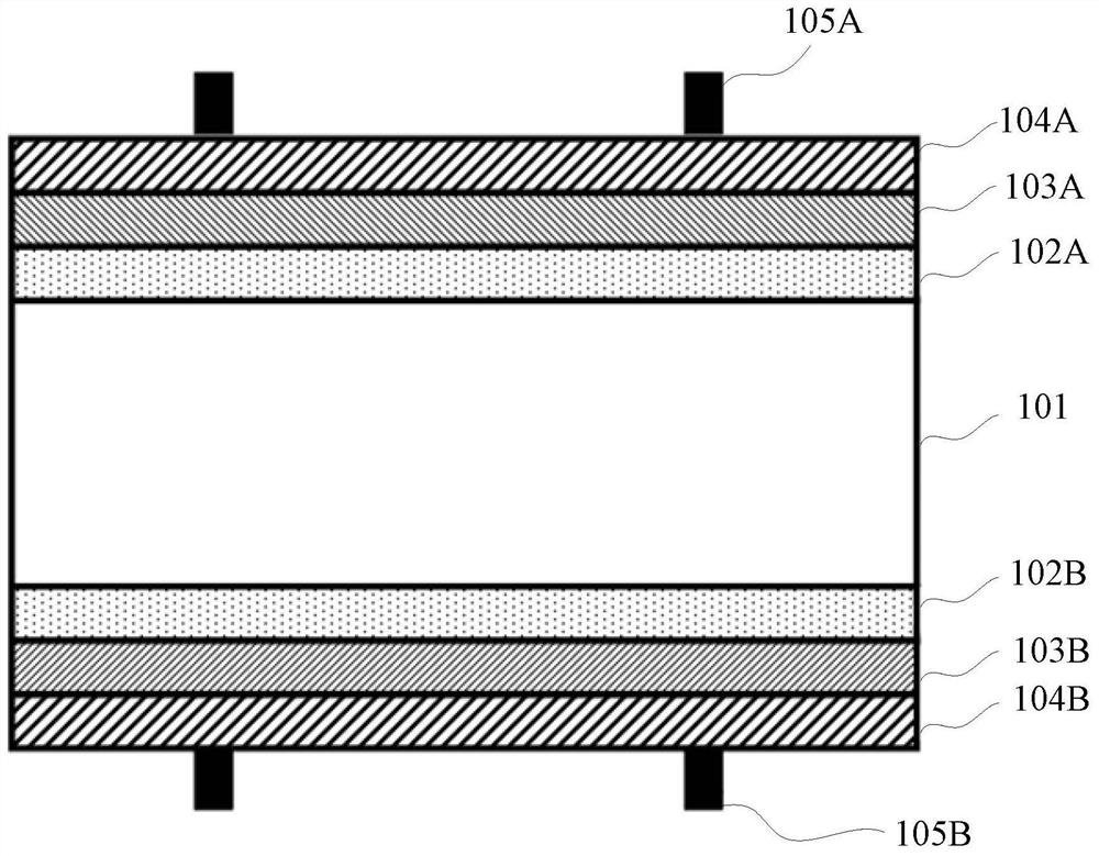
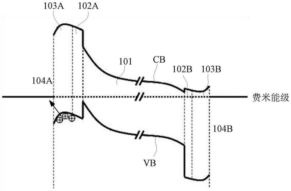
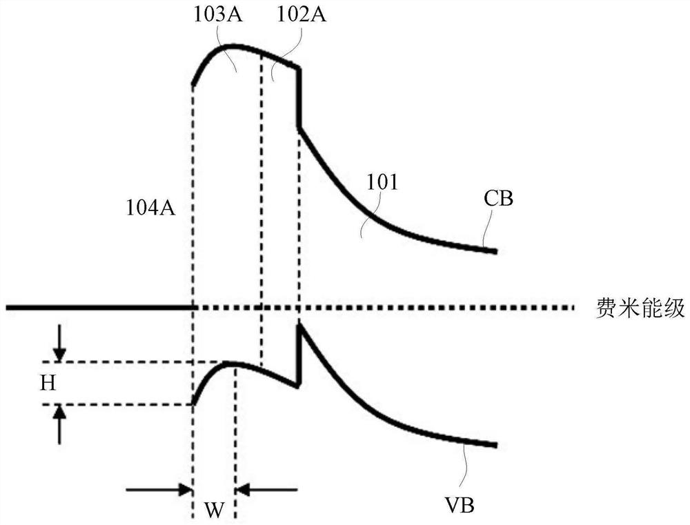
[0039] Hereinafter, embodiments of the present disclosure will be described with reference to the drawings. It should be understood, however, that these descriptions are exemplary only, and are not intended to limit the scope of the present disclosure. Also, in the following description, descriptions of well-known structures and techniques are omitted to avoid unnecessarily obscuring the concepts of the present disclosure.

[0040] Various structural schematic diagrams according to embodiments of the present disclosure are shown in the accompanying drawings. The figures are not drawn to scale, with certain details exaggerated and possibly omitted for clarity of presentation. The shapes of the various regions and layers shown in the figure, as well as their relative sizes and positional relationships are only exemplary, and may deviate due to manufacturing tolerances or technical limitations in practice, and those skilled in the art will Regions / layers with different shapes, ...


PUM

PropertyMeasurementUnit
thicknessaaaaaaaaaa

Abstract

The invention discloses a silicon heterojunction cell and a manufacturing method thereof, relates to the technical field of solar cells, and aims to reduce a Schottky barrier between a P-type doped silicon layer and a transparent conductive layer and reduce the width of a depletion layer of the P-type doped silicon layer so as to improve the hole collection capability and improve the cell performance. The silicon heterojunction cell comprises a silicon substrate, an interface inversion layer and a first transparent conductive layer. The silicon substrate includes a doped silicon substrate, a P-type doped silicon layer, and a first intrinsic silicon layer formed between the doped silicon substrate and the P-type doped silicon layer. The interface inversion layer is formed on the P-type doped silicon layer. The first transparent conductive layer is formed on the interface inversion layer. The interface inversion layer contains polar organic molecules. The polar organic molecules are bonded with silicon atoms in the P-type doped silicon layer. The interface inversion layer has a dipole moment pointing from the transparent conductive layer to the P-type doped silicon layer. The manufacturing method of the silicon heterojunction battery is used for manufacturing the silicon heterojunction battery. The silicon heterojunction battery provided by the invention is used for photovoltaicpower generation.

Description

technical field [0001] The invention relates to the technical field of solar cells, in particular to a silicon heterojunction cell and a manufacturing method thereof. Background technique [0002] Silicon heterojunction (SHJ for short) solar cell is a cell structure with simple manufacturing process, high open circuit voltage, high conversion efficiency, low temperature coefficient, and no light-induced attenuation. Attention has become a popular development direction of high-efficiency solar cell technology. [0003] When the existing SHJ battery is in working condition, the N-type crystalline silicon substrate absorbs photons and generates electron-hole pairs, and the holes pass through the first intrinsic passivation layer and the P-type doped layer into the first transparent conductive layer for hole collection. , and collected by the metal electrode, the electrons pass through the second intrinsic passivation layer and the N-type doped layer into the second transparent...

Claims


Application Information

Patent Timeline
Patent Type & Authority Applications(China)
IPC IPC(8): H01L31/0747H01L31/0224H01L31/20H01L31/0352
CPCH01L31/202H01L31/0747H01L31/022425H01L31/03529Y02E10/50
Inventor 徐琛
Owner LONGI GREEN ENERGY TECH CO LTD
Why Eureka
Try Eureka