RC-IGBT device with collector polysilicon electronic channel
An electronic channel and collector technology, applied in electrical components, semiconductor devices, circuits, etc., can solve the problems of hindering electron movement and long turn-off time, and achieve the effect of eliminating the snapback effect.
- Summary
- Abstract
- Description
- Claims
- Application Information
AI Technical Summary
Problems solved by technology
Method used
Image


Examples
Embodiment 1
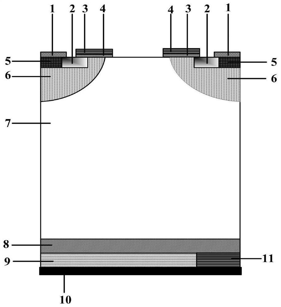
[0040] Such as figure 2 As shown, a preferred RC-IGBT device with a collector polysilicon electron channel in the embodiment of the present invention includes a set top semiconductor region: emitter 1, N+ electron emitter 2, gate 3, gate oxide layer 4, P+ Emitter 5, P-body 6, N-type drift region 7; collector region includes from left to right: buffer layer 8, P+ hole region 9, metal collector 10, N-collector 11, n-type polysilicon 12, P Type electron blocking layer 13.
[0041] The P-type electron blocking layer 13 is located on the right side of the P+ hole region 9 and has a distance L from the right edge of the device. The upper surface of the n-type polysilicon is in contact with the N-collector 11, the P+ hole region 9, the P-type electron blocking layer 13, and the buffer layer 8 respectively from left to right.
[0042] The P+ hole region 9 is flush with the lower surface of the N-collector 11 , and the rest of the N-collector 11 is completely covered by the P+ hole ...
Embodiment 2
[0047] Such as image 3 As shown, a preferred RC-IGBT device with a collector polysilicon electron channel in the embodiment of the present invention, on the basis of Embodiment 1, the P-type electron blocking layer 13 is moved upward, so that the P-type electron blocking layer 13 is left The side is adjacent to the P+ hole region 9, the right side is a certain distance from the right edge of the device, and the lower surface is also a certain distance from the upper surface of the n-type polysilicon 12. The P-type electron blocking layer 13 has a length of 22 μm, a thickness of 1.5 μm, and a doping concentration of 1×10 17 cm -3 .
Embodiment 3
[0049] Such as Figure 4 As shown, an RC-IGBT device with a collector polysilicon electronic channel is preferred in the embodiment of the present invention. On the basis of Embodiment 1, the drift region is replaced by alternately arranged P-type and N-type columns to form a super junction structure , The superjunction power device drift region is composed of mutually stacked and overlapping P-type and N-type doped columns, which extend from the drift region to the anode and cathode, and the height of these columns is consistent with the thickness of the drift region. The P-type electron blocking layer 13 has a length of 22 μm, a thickness of 1.5 μm, and a doping concentration of 1×10 17 cm -3 .
[0050] With the help of MEDICI simulation software, the figure 1 The conventional RC-IGBT shown, figure 2 An RC-IGBT with a polysilicon electronic channel is shown, Figure 6 shown in the AB RC-IGBT and Figure 7 The FPL RC-IGBT shown is simulated for comparison. During the ...
PUM
| Property | Measurement | Unit |
|---|---|---|
| length | aaaaa | aaaaa |
| thickness | aaaaa | aaaaa |
| length | aaaaa | aaaaa |
Abstract
Description
Claims
Application Information
 - R&D
- Intellectual Property
- Life Sciences
- Materials
- Tech Scout
- Unparalleled Data Quality
- Higher Quality Content
- 60% Fewer Hallucinations
Browse by: Latest US Patents, China's latest patents, Technical Efficacy Thesaurus, Application Domain, Technology Topic, Popular Technical Reports.
© 2025 PatSnap. All rights reserved.Legal|Privacy policy|Modern Slavery Act Transparency Statement|Sitemap|About US| Contact US: help@patsnap.com