Polycrystalline silicon material filling method in semiconductor device structure and preparation method of 3D NAND memory
A 3DNAND, device structure technology, applied in semiconductor devices, electric solid state devices, electrical components, etc., can solve problems affecting device performance, film formation effects, arc effects, etc.
- Summary
- Abstract
- Description
- Claims
- Application Information
AI Technical Summary
Problems solved by technology
Method used
Image
Examples
Embodiment 1
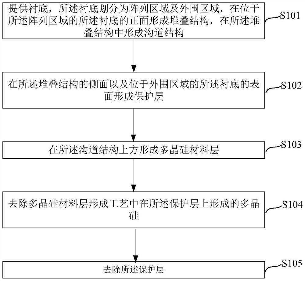
[0096] This embodiment provides a polysilicon material filling method in a semiconductor device structure, such as image 3 As shown, the method includes the following steps:
[0097] S101: Provide a substrate, the substrate is divided into an array area and a peripheral area, a stack structure is formed on the front surface of the substrate located in the array area, and a channel structure is formed in the stack structure;
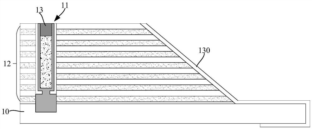
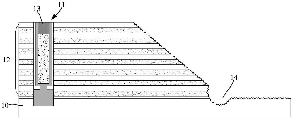
[0098] The aforementioned semiconductor device structure may be various semiconductor device structures that require the formation of polysilicon material layers or polysilicon contact plugs and other similar structures. In this embodiment, a 3D NAND memory is taken as an example for illustration. It should be understood that the 3D NAND memory is only exemplary and not limiting.
[0099] like Figure 4 As shown, a substrate 101 is provided, and the substrate 101 may be any suitable substrate such as a silicon substrate, a silicon-on-insulator substrat...
Embodiment 2
[0118] This embodiment provides a method for preparing a 3D NAND memory, such as Figure 12 As shown, the method includes the following steps:
[0119] S201: Provide a substrate, the substrate is divided into an array area and a peripheral area;
[0120] S202: Alternately stack sacrificial layers and insulating layers on the front surface of the substrate located in the array area to form a stack structure, the stack structure includes a core area and a step area;
[0121] S203: forming a channel hole in the core region, forming a memory layer and a channel layer in sequence on the sidewall of the channel hole, and filling a dielectric layer in the middle of the channel hole;
[0122] S204: Forming a protection layer on the surface of the step region of the stack structure and the substrate located in the peripheral region;
[0123] S205: forming a polysilicon plug on the top of the channel hole;
[0124] S206: Removing the polysilicon formed on the protective layer during ...
PUM
 Abstract
Description
Claims
Application Information
 - R&D
- Intellectual Property
- Life Sciences
- Materials
- Tech Scout
- Unparalleled Data Quality
- Higher Quality Content
- 60% Fewer Hallucinations
Browse by: Latest US Patents, China's latest patents, Technical Efficacy Thesaurus, Application Domain, Technology Topic, Popular Technical Reports.
© 2025 PatSnap. All rights reserved.Legal|Privacy policy|Modern Slavery Act Transparency Statement|Sitemap|About US| Contact US: help@patsnap.com


