Current bias circuit for quickly waking up chip

A technology of current bias and bias current, which is applied in the direction of adjusting electrical variables, instruments, control/regulation systems, etc., and can solve problems such as long chip wake-up time

Active Publication Date: 2021-03-09
BEIJING SMARTCHIP MICROELECTRONICS TECH COMPANY +3
View PDF8 Cites 0 Cited by
  • Summary
  • Abstract
  • Description
  • Claims
  • Application Information

AI Technical Summary

Problems solved by technology

[0004] The purpose of the present invention is to provide a current bias circuit for quickly waking up the chip to quickly start the key circuits in the chip, thereby solving the problem of long wake-up time of the chip

Method used


Image

  • Current bias circuit for quickly waking up chip
  • Current bias circuit for quickly waking up chip
  • Current bias circuit for quickly waking up chip

Examples


Embodiment Construction

[0019] Specific embodiments of the present invention will be described in detail below in conjunction with the accompanying drawings. It should be understood that the specific embodiments described here are only used to illustrate and explain the present invention, and are not intended to limit the present invention.

[0020] In the embodiments of the present invention, the terms "first", "second", "third", "fourth" and so on are only used for distinguishing descriptions, and should not be understood as indicating or implying relative importance.

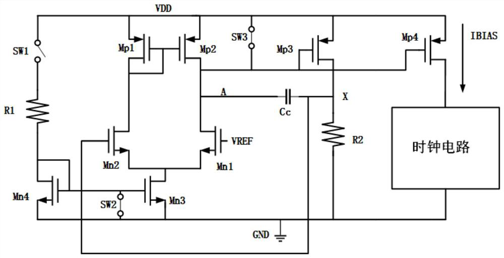
[0021] figure 1 It is a circuit diagram of an existing current bias circuit in a normal working state. like figure 1 As shown, the existing current bias circuit includes a bias current generating circuit, a low-precision bias current generating circuit and a current output branch. The bias current generation circuit includes: a first PMOS transistor Mp1, a second PMOS transistor Mp2, a first NMOS transistor Mn1, a second NMOS tra...


PUM


Abstract

The invention provides a current bias circuit for quickly waking up a chip, which belongs to the technical field of integrated circuits. The current bias circuit comprises a bias current generation circuit, a low-precision bias current generation circuit, a current output branch and an additional switch circuit. The additional switch circuit is arranged between the bias current generation circuitand the current output branch and is used for instantly lowering the potential of a working point of the current output branch in the process that the current bias circuit is turned off to be turned on; therefore, the current output branch is rapidly opened to output the bias current generated by the bias current generation circuit. The potential of the working point of the current output branch is instantly lowered by the additional switch circuit in the process of switching off the current bias circuit to switching on the current bias circuit, so that the current output branch is quickly switched on to output bias current, and various key circuits in the chip are quickly started to quickly wake up the chip; and the problem of long chip awakening time is solved.

Description

technical field [0001] The invention relates to the technical field of integrated circuits, in particular to a current bias circuit for quickly waking up a chip. Background technique [0002] Most chips used in the Internet of Things, industrial control, communication and other fields need to have multiple working modes to meet the low power consumption requirements in battery-powered and wireless power supply scenarios. Most of the time the chip is in sleep mode, and most circuits in the chip are turned off to reduce power consumption and loss. When the chip is triggered by a wake-up source, it enters the normal working state, and re-enters the sleep state after completing related tasks to save power consumption. When the chip wakes up, its internal voltage reference, oscillator circuit, clock circuit, phase-locked loop and other high-precision circuits need accurate bias current when starting from the off state, and the bias circuit that generates the bias current also ne...

Claims


Application Information

Patent Timeline
Patent Type & Authority Applications(China)
IPC IPC(8): G05F1/56
CPCG05F1/56
Inventor 胡毅唐晓柯王于波侯佳力冯文楠张帆
Owner BEIJING SMARTCHIP MICROELECTRONICS TECH COMPANY
Why Eureka
Try Eureka