Manufacturing method of GOI test sample wafer for improving breakdown characteristic of trench gate

A manufacturing method and technology of breakdown characteristics, applied in semiconductor/solid-state device manufacturing, electrical components, semiconductor devices, etc., can solve problems such as electric field concentrated breakdown, test result interference, etc.

Pending Publication Date: 2021-03-05
ZHUZHOU CRRC TIMES SEMICON CO LTD
View PDF9 Cites 0 Cited by
  • Summary
  • Abstract
  • Description
  • Claims
  • Application Information

AI Technical Summary

Problems solved by technology

In the manufacturing process of trench IGBT, the top of the trench is usually sharp, which causes the electric field on the top of the trench to break down, thereby introducing defects and disturbing the actual test results.

Method used


Image

  • Manufacturing method of GOI test sample wafer for improving breakdown characteristic of trench gate
  • Manufacturing method of GOI test sample wafer for improving breakdown characteristic of trench gate
  • Manufacturing method of GOI test sample wafer for improving breakdown characteristic of trench gate

Examples


Embodiment 1

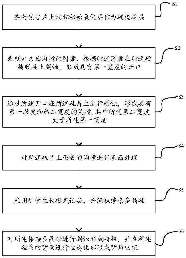
[0031] see figure 1 , the present embodiment proposes a method for manufacturing a GOI test sample to improve the breakdown characteristics of the trench gate, which specifically includes the following steps:

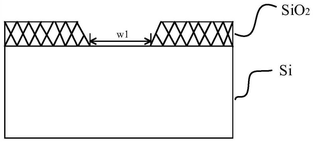
[0032] S1: An initial oxide layer is deposited on the substrate silicon wafer as a hard mask layer.

[0033] The substrate silicon wafer in the present invention can be an N-type substrate or a P-type substrate, and in this embodiment, it is preferably an N-type substrate.

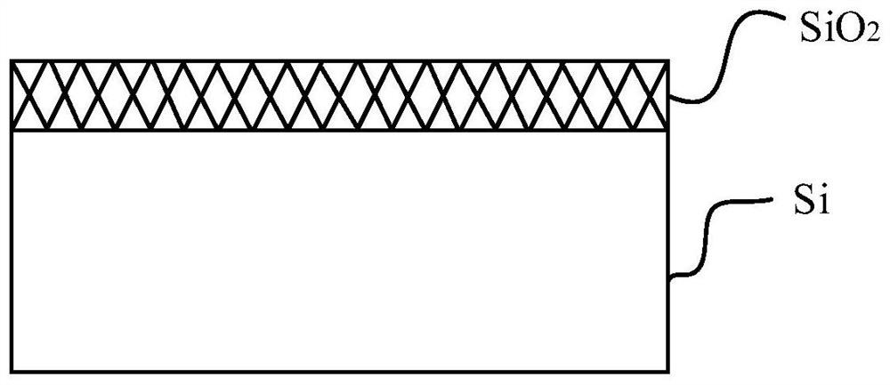
[0034] The initial oxide layer in the present invention is insulating material SiO 2 , used to protect the internal substrate silicon wafer and realize the surface insulation function, the substrate silicon wafer is Si, such as figure 2 shown.

[0035] The method for depositing the initial oxide layer in the present invention is not limited to oxidation methods such as wet oxygen, dry oxygen, and chlorine-doped oxidation. In order to reduce the front oxidation rate, the thickness of the initial...


PUM


Abstract

The invention provides a manufacturing method of a GOI test sample for improving breakdown characteristics of a trench gate. The method comprises the following steps: S1, depositing an initial oxide layer on a substrate silicon wafer to serve as a hard mask layer; S2, performing photoetching to define a pattern of a groove, and performing etching on the hard mask layer according to the pattern toform an opening with a first width, wherein the first width is the distance of the opening in a direction parallel to the silicon wafer; S3, performing etching on the silicon wafer through the openingto form a groove with a first depth and a second width, wherein the second width is larger than the first width; S4, carrying out surface treatment on the groove formed in the silicon wafer; S5, growing a gate oxide layer by adopting a furnace tube, and depositing a conductive medium on the gate oxide layer; and S6, etching the doped polycrystalline silicon to form a grid electrode, and metallizing the back surface of the silicon wafer to form a back surface electrode.

Description

technical field [0001] The invention relates to the technical field of semiconductor manufacturing, in particular to a method for manufacturing a GOI test sample that improves the breakdown characteristics of trench gates. Background technique [0002] IGBT power device is a new type of power semiconductor device with rapid development and wide application. It is based on ordinary double diffused metal oxide semiconductor (DMOS), by introducing P+ structure in the collector, in addition to DMOS high input impedance, fast switching speed, high operating frequency, easy voltage control, good thermal stability, drive In addition to the characteristics of simple circuit and easy integration, the on-resistance and on-state power consumption are greatly reduced through the conductance modulation effect of collector hole injection. At present, power IGBT has been widely used in frequency conversion home appliances, wind power generation, locomotive traction, smart grid and other f...

Claims


Application Information

Patent Timeline
Patent Type & Authority Applications(China)
IPC IPC(8): H01L21/28H01L21/033
CPCH01L21/28211H01L21/28238H01L21/0332
Inventor 唐云罗海辉谭灿健罗湘杜龙欢刘少杰刘斌易彬
Owner ZHUZHOU CRRC TIMES SEMICON CO LTD
Why Eureka
Try Eureka