
Holographic information layer, anti-counterfeiting film and identification assembly

A technology of holographic information and anti-counterfeiting film, applied in the field of anti-counterfeiting printing, can solve problems such as short lifespan

Pending Publication Date: 2021-03-02
WUHAN HUAGONG IMAGE TECH & DEV
View PDF6 Cites 0 Cited by
  • Summary
  • Abstract
  • Description
  • Claims
  • Application Information

AI Technical Summary

Problems solved by technology

The image of the current holographic anti-counterfeiting pattern is easy to separate and has the problem of short life

Method used


Image

  • Holographic information layer, anti-counterfeiting film and identification assembly
  • Holographic information layer, anti-counterfeiting film and identification assembly
  • Holographic information layer, anti-counterfeiting film and identification assembly

Examples


Embodiment 1

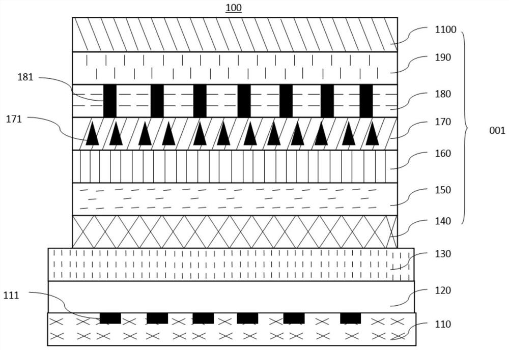
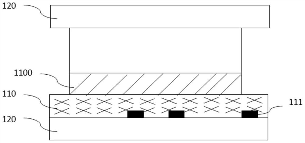
[0048] figure 1 A schematic structural view of the anti-counterfeiting film 100 provided by the embodiment of the present application is shown, figure 2 show figure 1 Sectional view along line AA, image 3 show figure 1 Sectional view along line BB; see Figure 1-Figure 3 , the present embodiment provides an anti-counterfeit film 100, the anti-counterfeit film 100 mainly includes a holographic information layer 001 and a base film 120; in the process of use, the adhesive layer 1100 of the anti-counterfeit film 100 is attached to objects such as cards; then the base film is separated 120. Leave the holographic information layer 001 on the surface of objects such as cards.

[0049] see figure 2 , the following is an example of the main structure of the holographic information layer 001.

[0050] The holographic information layer 001 mainly includes a base layer 150 , an imaging layer 170 , a coating layer 180 and an adhesive layer 1100 which are sequentially stacked. Th...

Embodiment 2

[0090] Figure 4 It shows a schematic cross-sectional view of the identification assembly 200 provided by the embodiment of the present application, please refer to figure 2 and Figure 4 Embodiment 2 provides an identification component 200. The identification component 200 includes a substrate 210 and a holographic information layer 001. For the specific structure of the holographic information layer 001, please refer to Embodiment 1, which will not be repeated in this embodiment.

[0091] The glue layer 1100 of the holographic information layer 001 is connected with the base body 210 .

[0092] It can be understood that the substrate 210 can be a card, a card, etc. The embodiment of the present application does not limit the material of the substrate 210, and the identification component 200 has all the advantages of the above-mentioned holographic information layer 001.

[0093] The adhesive layer 1100 has good adhesion to the substrate 210, and the inside of the hologr...


PUM

PropertyMeasurementUnit
Sizeaaaaaaaaaa
Diameteraaaaaaaaaa
Thicknessaaaaaaaaaa

Abstract

The invention relates to the field of anti-counterfeiting printing, in particular to a holographic information layer, an anti-counterfeiting film and an identification assembly. The holographic information layer comprises a base layer, an imaging layer, a plating layer and an adhesive layer which are stacked in sequence; the imaging layer is provided with holographic patterns; the plating layer isprovided with a plurality of through holes penetrating through the plating layer in the thickness direction. The size of the through hole is smaller than 250 microns; the distance between every two adjacent through holes is larger than or equal to 500 microns. And the through holes are filled with a binder, and the binder is used for bonding the plating layer and the imaging layer. The holographic patterns in the imaging layer cannot disappear due to the arrangement mode of the through holes in the plating layer; binding agents used for bonding the plating layer and the imaging layer are arranged in the through holes, the binding agents in the through holes can further improve the adhesive force between the plating layer and the layer structure on the side away from the imaging layer, andthe problem that the imaging layer and the plating layer are prone to separation due to large material difference is effectively solved.

Description

technical field [0001] This application relates to the field of anti-counterfeiting printing, in particular, to a holographic information layer, an anti-counterfeiting film and an identification component. Background technique [0002] The means of card anti-counterfeiting is to use chips, and the other is to use holographic anti-counterfeiting. There are two types of card holographic anti-counterfeiting. One is to prepare the holographic anti-counterfeiting pattern inside the card during the card making process, and the second is to attach the holographic anti-counterfeiting pattern to the surface of the card after the card is made. The image of the current holographic anti-counterfeiting pattern is easy to separate and has the problem of short service life. Contents of the invention [0003] The purpose of the embodiment of the present application is to provide a holographic information layer, an anti-counterfeiting film and a label component, which aims to improve the ...

Claims


Application Information

Patent Timeline
IPC IPC(8): G09F3/02G09F3/10
CPCG09F3/0294G09F3/10G09F2003/0257
Inventor 石建行杨志方周聪申政徐晓光
Owner WUHAN HUAGONG IMAGE TECH & DEV
Learn More